10 MHz
Double Redundant Quad Distribution Amplifier
This page
details my work to provide a redundant medium quality 10 MHz signal source for
use in future projects and general purpose testing
Last
updated:
·
2015-05-25:
Initial publication
Contents
Figur
1 - My example application
Figur 3 - Clock detection circuit
Figur 5 - 3D render of top layer
Figur 6 - 3D render of bottom layer
The
problem
RF systems
and precision measurements usually require a stable frequency reference to
generate accurate RF carriers or to accurately measure the carriers generated.
I currently
have a D-Star repeater running at home using converted NMT 450 base station
equipment, the transmitter and receiver use TCXOs as a time base reference,
each unit needs to be calibrated periodically to hit the narrow band carriers
in D-Star.
I plan to
replace the synthesizers in these units with a custom design, since they
currently use modified (hacked more like) synth boards that aren’t likely to be
reliable long term, I intend to build these units to accept 10 MHz inputs as synth references to remove the need for
calibrations.
I have a
Z3810AS GPS timing system, which includes two OCXO units controlled by GPS, the
system has a 15 MHz output (redundant) and each unit has a 10 MHz test point
(lower quality, more phase noise). We’ll pretend we can convert the 15 MHz to a
more useful 10 MHz, in that case a device is needed to preferably use the 15
MHz derived signal as the time base.
If this
disappears (power failure will cause the 15 MHz to be disabled until a lock is
attained) then we may want to use one of the 10 MHz test points.
In the
Z3810AS system the secondary unit which locks onto GPS first will be more
reliable during startup, so we want to use the 10 MHz output from that unit as
the secondary source until the 15 MHz is enabled once the system reaches a
certain accuracy. We may alternately use a completely different source for the
secondary, such as a rubidium oscillator or stable OCXO/TCXO.
In the case
of complete failure of the Z3810AS or its power supply both signals will
disappear, in this case we want a second redundancy that can provide a degraded
but usable 10 MHz, for example a low cost TCXO.
The
solution
To ensure
reliable performance I decided to build a distribution amplifier that support
redundant inputs with automatic switching to ensure these radios always receive
the most reliable frequency source available. This amplifier has two inputs +
an internal oscillator.
Each input
+ the internal signal is fed to a 74HC125 tri state buffer with separate enable
signals, one of these is activated based on a priority encoder and the winning
signal is fed to a 74HC14 driver IC that drives four outputs with a 50 ohm
series terminated AC coupled CMOS output signal.
To detect
loss of signal two 7474 latches are clocked from the internal clock, if the
input clock is stuck in any state for more than two cycles this will be
detected by the two latch chains, a NAND gate combines the signals to one
output. This circuit is repeated for input 2, these two outputs then indicate
the status of the clock inputs, and are fed to a priority encoder configured to
choose input 1, then input 2, then internal clock if all else fails.
If an input
is lost the circuit will switch inside of 2-3 cycles of 10 MHz, ensuring
minimal disruption. If both external sources are lost it will switch to the
internal reference until one of the other sources are reliable, ensuring some
sort of 10 MHz source is always present.
Typical
application
My
particular application for this design is as follows:
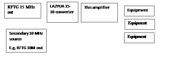
Figur 1 - My example application
We assume
the 15-10 MHz converter is present and working, in this case a failure of one
of the RFTG units will cause the other to take over in providing 15 MHz, therefore
we have redundancy into the 15-10 converter. If the RFTG system is reset then
the 15 MHz is disabled until it reaches around 1 ppb or better and GPS lock is
attained, in that time period there will be no signal from the 15-10 converter.
The Ref-1 unit in the RFTG will reach a stable frequency faster (but will not
be as short term accurate after full lock is attained), so we use that as the
secondary input.
If the RFTG
fails completely, for example a bad power supply, then the internal TCXO takes
over and we may continue operation with reduced accuracy (~1 ppm or so,
compared to around 1x10^-12 as is typical from a GPSDO).
This system
therefore can handle three failures (hard reset of RFTG, failure of one RFTG
unit or complete failure of both RFTGs) without failure of the output, the
system as configured may therefore be called triple redundant by some
definitions.
By adding a
third source (external OCXO/LPRO) the system can truly be triple redundant,
however a single failure point exists in the internal timebase.
Circuit
descriptions
Input
stage
Each
external input is transformer coupled and 50 ohm terminated, the center tap on
the secondary is used to set the common mode voltage to half the supply rail.
The
balanced signal is fed to the inputs of an LT1713 high speed comparator, the Q
output is used for the tri state buffer and the Qbar output is connected to the
clock detection circuitry. This reduces the load on the Q output where signal
fidelity matters.
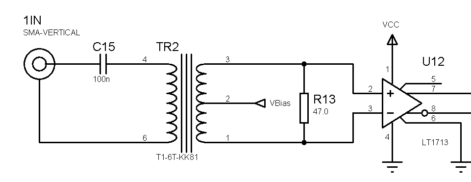
Figur 2 - Input stage
The LT1713
is not ideal wrt. jitter but it is relatively available and simple, as the
clock signal must also pass through standard 74 series logic it’s not a huge
loss in fidelity.
Clock
detection
The clock
detection works by clocking two D latches from the reference clock and wiring
the external clock to the Set port, in this case if the external clock is stuck
high for two cycles of INTOSC the zero from the first latch will flow through
the latch and the output will change state. The circuit is repeated with an
inverter to check for stuck low situations and a NAND gate checks that both
chains are set correctly.
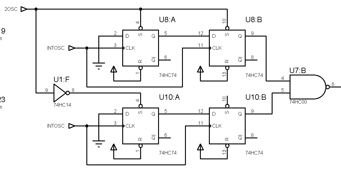
Figur 3 - Clock detection circuit
Output
driver
Each output
port has a 74HC14 driver with 22 ohm in series and a basic edge shaving filter
to reduce EMI. It is assumed that the high frequency output impedance of the
7414 is relatively high.
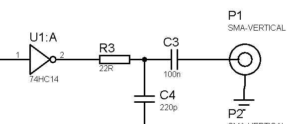
Figur 4 - Output driver
Test
results
Stay tuned,
still testing.
I intend to
check this design for added phase noise using a spectrum analyzer and a pure
signal source.
Schematic,
PCB layout
The
schematic, BOM and gerber files can be found here:
Notes:
BOM error,
transformer is Mini-Circuits, not Magnecraft
PCB layout:
please note that the top layer of the PCB is a power plane, the ground plane is
on the bottom layer. The mounting holes are connected to ground.
74 logic
family: higher speed ICs are generally better wrt. jitter, for U2 and U1 use
only CMOS types: HC, AC or better.
HC or better is recommended for all other ICs to
reduce power consumption but is not required
Assembly
notes:
None in
particular, socketing the internal reference may be advantageous, but also
increases the chance that it will fall out or develop a bad contact later. I
recommend using a TCXO instead of a standard crystal oscillator to improve
performance if you expect the external signals to disappear.
Here are 3D
renders of the top and bottom layers:
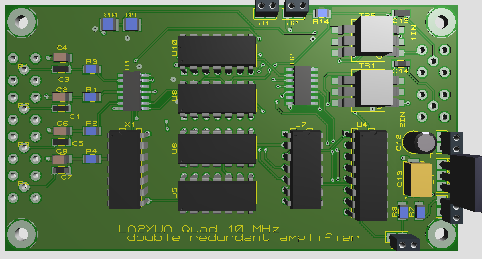
Figur 5 - 3D render of top layer
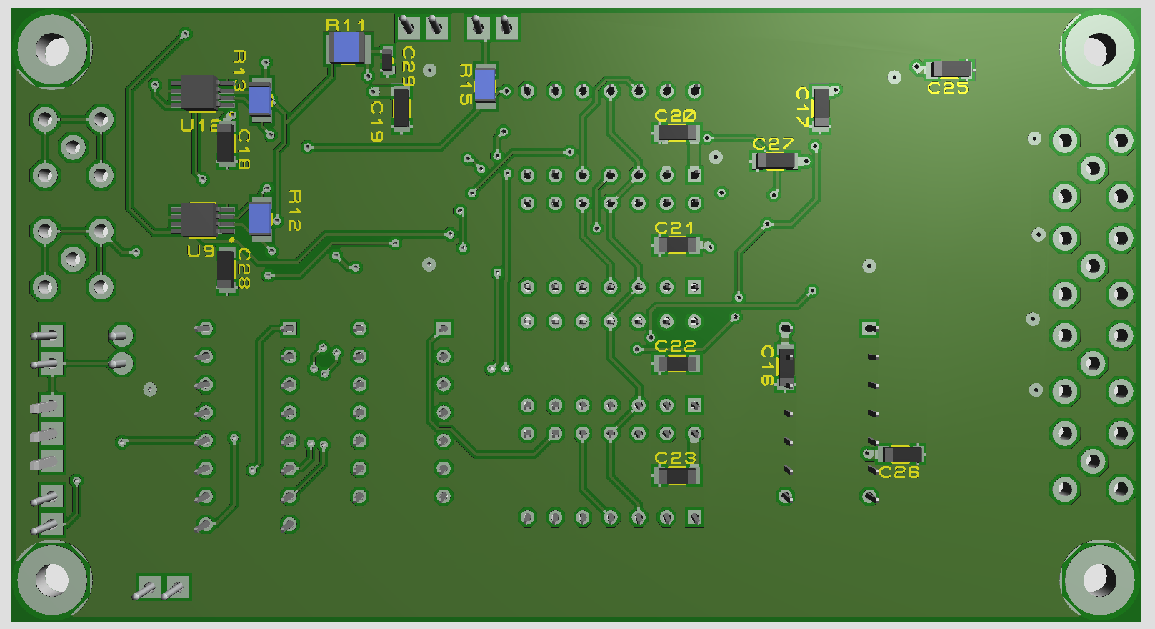
Figur 6 - 3D render of bottom layer