HP 5335A
Universal Counter RF Prescaler (Option 030)
replacement
This page
details my work to upgrade my HP 5335A universal counter with the Option 030 RF
prescaler.
Last
updated:
·
2015-05-25:
Initial publication
Please
note: there are two versions of this type of board, I’m redesigning the older
version which uses an oddball divide by 20 circuit, later versions apparently
used a divide by 32 or 64, this board will not work
for those versions.
Contents
Figur 1 - 5335A showing a 10 MHz
signal
Figur 2 - Option 030 block diagram
Figur 3 - HP option 030 schematic
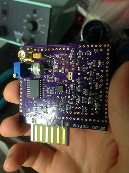
Figur 4 - Option 030 Assembly Picture
Figur 5 - Revision A block diagram
Figur
7 - Revision A testing showing 2.8 GHz.
Figur 8 - 3D render of 5335A O030
rev B
Figur 9 - Option 030 front panel
5335A
overview
The 5335A is
a fairly sophisticated frequency counter with a lot of extra features, the
version I have comes with a fairly basic kit.
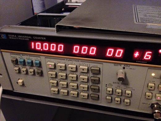
Figur 1 - 5335A showing a 10 MHz signal
The standard
version has two 150 MHz inputs with a fairly standard oscilloscope style input
set, 1M/50 ohm input impedance, AC/DC coupling and adjustable trigger levels.
By default
you will measure frequencies with it on channel A,
channel B is usually not used and can’t be used to measure frequencies
directly.
A basic
arithmetic set can be enabled on measurements, offset, scaling, normalizing
etc. are supported and can be used to make the instrument display readings in
ppm, with relative frequencies etc.
Channel B
can be used to measure timing between two events, for example time from pulse
on A to B or frequency of A/B.
A neat
feature of the 5335A is the automatic switchover from frequency to on-time
measurement which means that unlike simpler instruments 1 Hz signals can be
measured with the same number of digits as a 10 MHz signal with the same gate
time. In frequency only instruments measuring slow signals with precision takes
a very long time since the instrument only displays the number of pulses
counted in the gate time, requiring a ridiculous gate time to measure slow
signals.
The service
manual is available online and has a lot of detail about the architecture of
the instrument.
Option
030, original
To support higher frequency measurements an
option board can be fitted, in this case option 030 which allows measurements
up to 1300 MHz.
Electrical
design
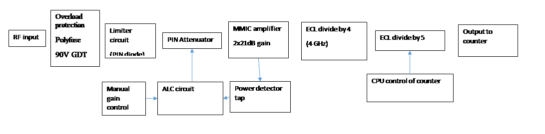
Here is
part of the system block diagram containing the prescaler:
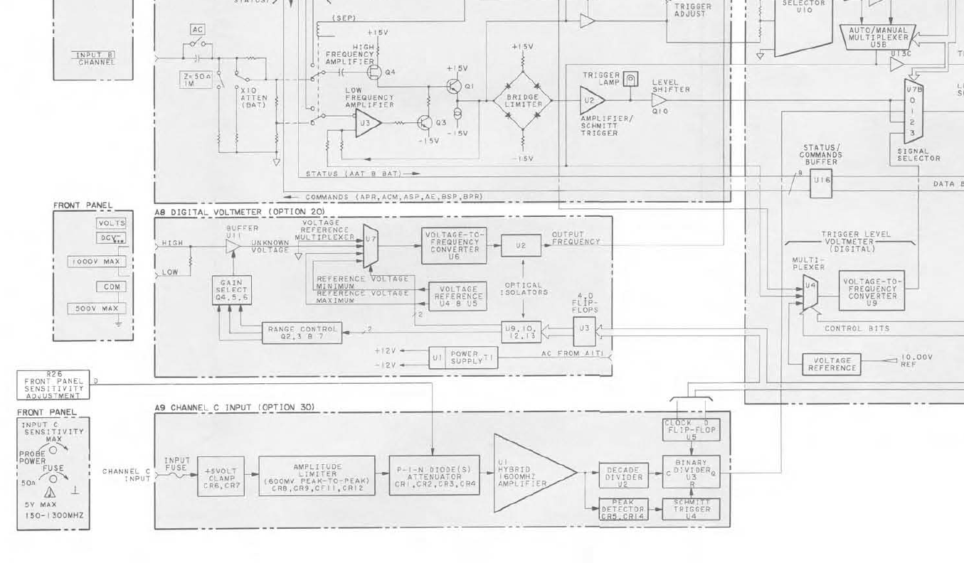
Figur 2 - Option 030 block diagram
As we can
see the RF input is called channel C, it contains fairly basic circuitry at the
block level, some basic levelling circuitry including an attenuator, an
amplifier and a divide by 20 circuit. The divider is implemented as a custom
divide by 10 IC and a standard ECL divide by 2. The divide by 2 is nominally
CPU controlled but I haven’t found any situations where that’s actually used to
I’ve left it out in revision B of my PCB as the counter will happily count
without it.
Here is the
original schematic:
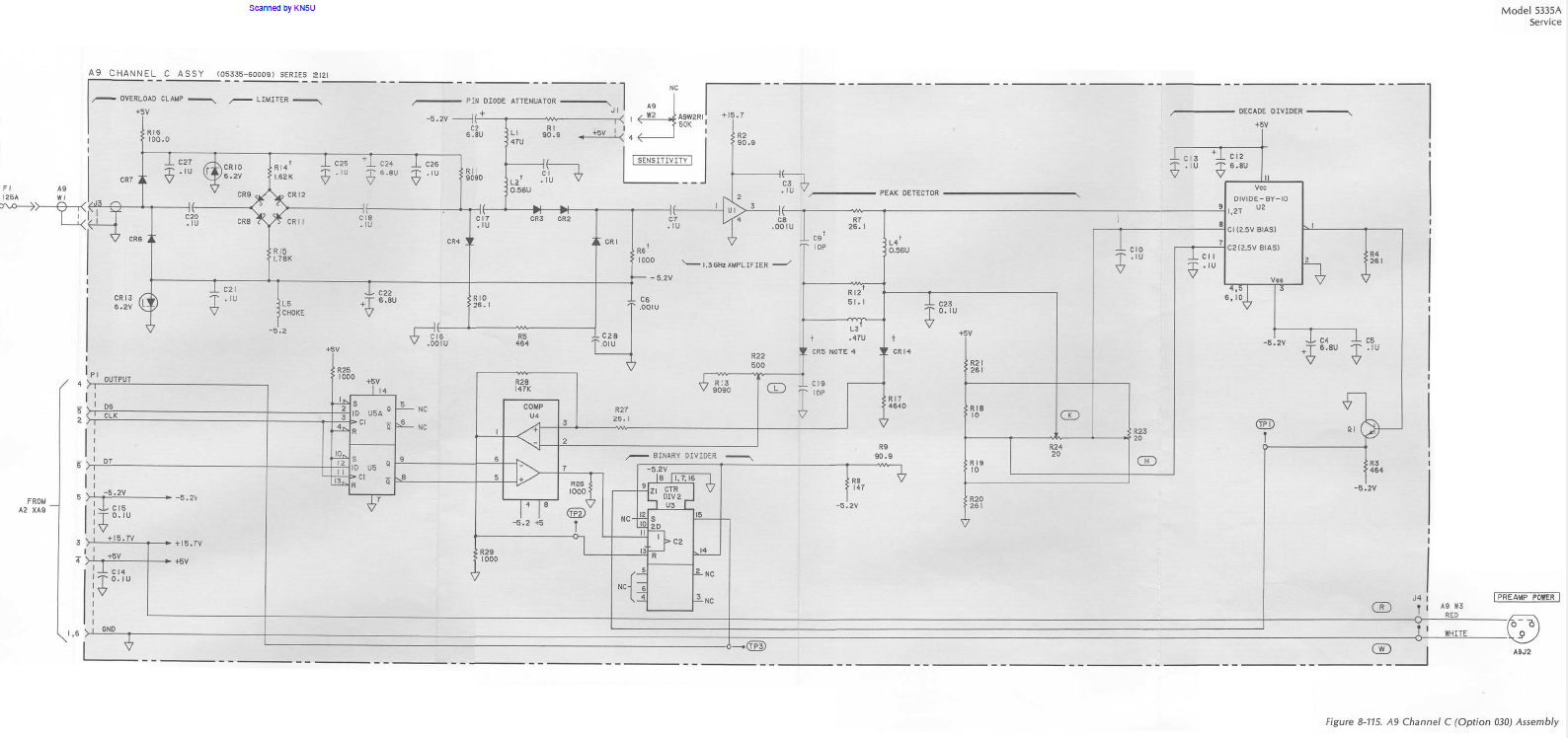
Figur 3 - HP option 030 schematic
The
original also included a power supply for an active probe, I will not be
implementing this, but adding this shouldn’t be a problem.
The entire
high speed and counting section is powered by NECL circuitry, the most interesting
parts are HP custom.
There’s
some other interesting parts of this design, we can see that this design is
limited by the 1600 MHz hybrid amplifier (a pretty old MMIC basically), at the
maximum input frequency the output to the counter is only running at around 65
MHz, we know the logic is capable of around 150 MHz.
This means that with modern circuitry this design could be capable of at least
doubling the RF frequency range supported.
I don’t have
a Option 030 board (if I did I would have used it
instead of making my own), but testing using a VHF radio transmitting into the
logic input of the counter showed it would definitely accept 150 MHz on the
input and correctly show 150*20 MHz on the display.
What is
certain is that this is enough information to redesign the PCB, almost all
parts will have to be replaced but we know we need a robust RF input, a divide
by 20 circuit with NECL outputs and a squelch.
Physical
design
I don’t
have the PCB I’m trying to redesign, but I do have a picture of the design:
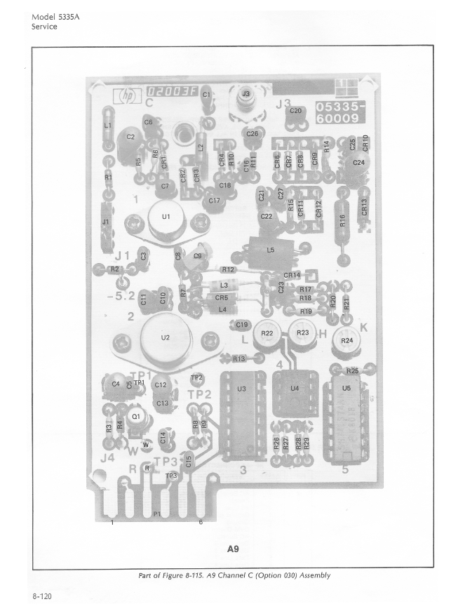
Figur 4 - Option 030 Assembly Picture
As we can
see it’s a double sided design, no doubt a beautiful gold finish with a SMB
connector going to the front panel.
A word of warning: there’s two 2x6 pin card edge connectors in
the counter, the one closest to the front panel is the option 030 slot, the
other is a slot for the DVM module, this contains a 24V AC supply that’s always
live. I suggest putting a piece of tape over this port unless you intend to use
it, connecting this board in that socket will destroy a very large amount of
TTL logic (ask me how I know) and it will take a long time to repair.
HP
helpfully provided the pinout but weren’t kind enough to describe the reverse
side of the connector so I had to measure my way to that:
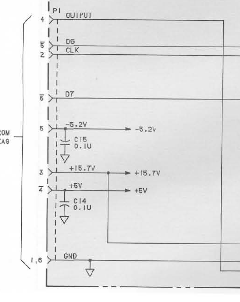
We can see
that all relevant supplies are available from the instrument.
Option
030, redesigned, rev A
My plan for
the new version of the O030 board was to use modern circuitry to improve performance
and reduce cost.
I built a
prototype PCB of revision A, testing showed reasonable
but not ideal performance. Specifically sensitivity was worse than desired (-30
dBm @ 280 MHz required no attenuation on the input)
and performance above 2 GHz was spotty.
Additionally
the lack of a squelch circuit meant that the counter would pick up anything in
the air and typically read 920 MHz whenever the input was floating, either
oscillation or GSM pickup.
Here’s the
basic block diagram, each section is separated with a 100 pF capacitor giving a
lower input range of around 100 MHz.
Figur 5 - Revision A block diagram
Overload
protection
The
overload protection is implemented with a 90V 15kA Gas Discharge Tube
immediately after the first AC coupling cap and a 150mA polyswitch
in series.
This has
not been properly tested, and the components have been replaced with lower
rated SMD versions in revision B.
Limiter
The limiter
circuitry uses a HSMP-4820 PIN diode from Avago in a self
biasing configuration, this will typically limit a +30dBm input signal
to around +15 dBm. This diode is supposed to conduct
enough to heat up the polyswitch in the overload
protection part if a severe overload is encountered.
PIN
attenuator
The PIN
attenuator uses 4 pin diodes in a pi configuration with a 1-15V control
voltage, the basis is Avago application note AN-1048. Attenuation range is
around 40 dB at GHz frequencies. The diode is a HSMP-3814 dual pin diode in
SOT-23.
MMIC
amplifier
The MMIC
amplifier is a composite amplifier using 2xABA-53563 MMIC amplifiers from
Avago, each amplifier can handle +20 dBm CW on the
input and provides 21 dB gain at 2 GHz with a P1dB of +13dBm below 2 GHz. Gain
is flat up to around 3.5 GHz.
These
amplifiers work well, a third amplifier was added in revision B to improve
sensitivity.
ECL
dividers
To support
the x20 divide ratio two dividers are used, the MC100EL33 is well suited to
this application and has balanced I/O with a bias pin built in to simplify
single ended inputs, it divides by 4 with a maximum of 4 GHz in. The MC100EP139
is a programmable divider, in this case it is configured for mod 5, it also has balanced I/O with multiple outputs.
The
dividers work well and have not been significantly changed in revision B,
however the original design used PECL, which required AC coupling on the
output. This was changed to use NECL in revision B since this is generally a
more robust way to use ECL and it simplifies interfacing to the rest of the
instrument.
Power
Tap and ALC
Originally
the circuit was supposed to detect the power level of the MMICs to allow an ALC
circuit to trim the gain control to keep them operating with lower distortion.
The detector never worked very well and this has been replaced in rev B with a
squelch circuit which might work. A LED is used to indicate the status of the
ALC/squelch.
The manual
gain control is connected to a trimmer on the front panel and buffered by a
TS912 opamp.
Prototype,
testing
A prototype
exists of revision A, here’s proof:
The
prototype was built and tested, aside from some issues with capacitors and opamps inserted backwards the design worked. Using the LO
out on my spectrum analyzer (around +10 dBm) I was
able to reach a maximum of 2.8 GHz.
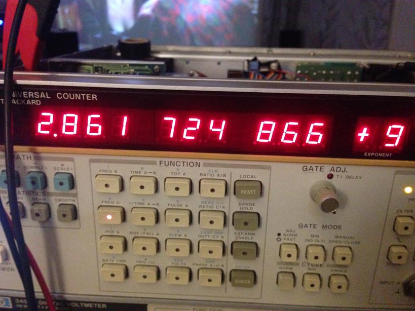
Figur 7 - Revision A testing showing 2.8
GHz
Several issues
were observed with the PECL/NECL conversion and with sensitivity in general, at
280 MHz/-30dBm the gain control must be set to maximum to get a stable reading.
Additionally
the ALC circuitry doesn’t work at all and has been disabled.
I used OSHPark for the prototype, the PCB quality is pretty good
and I have no complaints, especially considering the low price.
Option
030, rev B
Revision B
is currently undergoing testing, here is a list of changes made:
·
Overload
protection now uses all SMD components to improve RF performance
·
Routing
improved in limiter and PIN attenuator section to improve performance
·
Third
MMIC amplifier added to improve sensitivity
o
High
speed schottky diode clamp added between 2nd
and 3rd amplifier to improve limiting (HSMS-2822)
·
Even
more vias added, don’t ask me how I managed to fit
them
·
Power
tap now uses ADL5501 true RMS detector IC to get a reliable reading of signal
levels going into the ECL dividers
o
Internal
trimmer now used to set squelch level based on the power detector reading,
squelching is achieved by setting the RESET of U6
·
CPU
control of counters removed to free up space
·
ECL
dividers now use the N5V2 rail for power
·
Status
LEDs added for all power supply rails
·
Polyfuses added for all power rails to prevent shorting
the instrument rails in case of failure on the board
When the
design has been tested I will post schematics, BOM and gerber
files for anyone to download and build.
Here is a
3D render of the PCB:
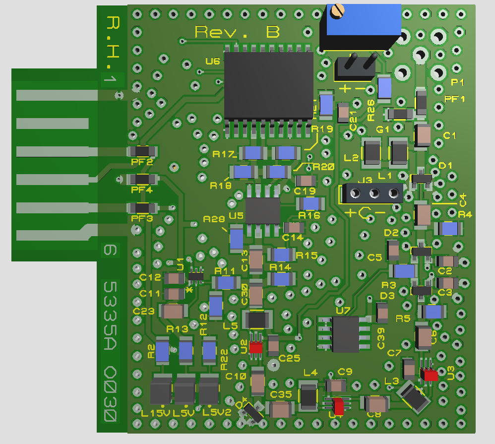
Figur 8 - 3D render of 5335A O030 rev B
Front
Panel
The front
panel section included in the default kit is a standard plate and it can be
removed by disassembling the front panel part of the counter. The internal aluminium frame has cutouts for all options so all we need
to do is drill holes at the right points.
I didn’t
get pictures of the inside but here’s my first attempt at a front panel:
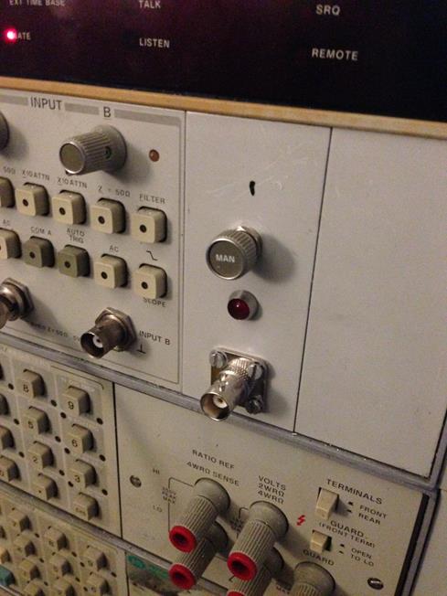
Figur 9 - Option 030 front panel
I later
replaced the knob with one salvaged from a HP spectrum analyzer module which is
larger and has labels from 0 to 12, corresponding roughly to the amount of
attenuation added.
The LED
indicates if the squelch is open.
The BNC
connector is a BNC-SMA adapter, a small SMA-SMA pigtail connects this to the
board inside the input.