

Magnetic AB/Ericsson NMT 450 transceiver system for Ham Radio
2017-06-10 – LA2YUA
This is a work in progress.
This is an
overview of my documentation for the Magnetic AB/Ericsson NMT 450 base station
transceiver system.
This
project started out as a simple “hack it to make it work” sort of job, which I
succeeded at in 2014. The receiver and transmitter were operational from 2014
to 2016 running an initial half-duplex D-Star repeater, then later a dual
antenna full duplex system.
My current
plan is to improve on this original system by reusing the better parts of the
system, and replacing the rest with custom designed circuitry to implement
either a very good 50W radio system, or a full duplex repeater stack suitable
for modern digital modes as well as high end analog performance.
Contents
Future plan: New 1st converter
Transmit Power Detector (TX Bridge)
CDCR83 RAMBUS clock generator as a local oscillator
CDCE913 based Local Oscillator
NMT 450 was
a fairly advanced 1G cellular phone network, operational from ca. 1981 to ~2004
or so though it was largely displaced by GSM networks by the late 90s. The
system replaced earlier “0G” networks such as OLT and an OLT like UHF system.
The system was a fully automatic roaming system using full duplex FM radios
operating in the 450 and 460 MHz bands with a 10 MHz duplex split. Deviation
was 5 kHz, as usual for FM systems of the era.
As shown
below the system used 180 channels with talk-in at the low side and BS TX at
the high side. The “UHF System” referred to in the figure is a manual UHF phone
network that I haven’t found much information about except for some fellow hams
mentioning it existed. This system was expected to be abandoned by 1987 to free
up the lower 80 channels for NMT use.
I suspect
that system was put in place as a stop gap measure due to a lack of channels
for the VHF OLT system in cities; with the introduction of 180 channels of NMT
along with what Ericsson proudly called the “small cell concept,” congestion
issues were FIXED FOREVER (until around 1985).
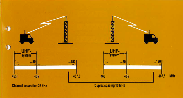
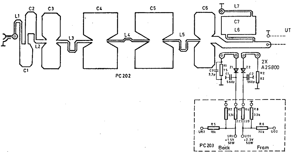
Figur 1 - NMT 450 channel concept
Mobile unit
power was up to 15W, while base stations had around 50W from each transmitter
with some combiner loss. A power reduction function was mandatory for mobile
units to reduce near-far interference, this was controlled by the base station
which would control a dedicated power measurement receiver to measure RF power
for each active channel in order to determine the required power level.
Interestingly,
the smallest NMT 450 phone ever built was a Nokia about the side of a 3210 (and
no, I’m not confusing it with NMT 900 phones, I actually have the 450 version
somewhere). Quite an achievement packing a sufficiently good band pass filter
into such a small package, but then nearly 20 years of development wasn’t for
nothing. Portable (as opposed to luggable) units were fortunately not required
to have 15W output power, though all other parameters would normally have to be
met.
A lot of
the original system documentation and requirement specifications are available
on the internet, such as here: http://download.eversberg.eu/mobilfunk/NMT-Dokus/
Allegedly
this system was the most advanced 1G network in the world when it was launched,
several features were new, including:
·
Automatic
dialing and channel selection
·
Automatic
billing
·
Automatic
handover
·
International
roaming (inside Scandinavia and neighboring countries; some countries that
later adopted the system could not roam to the Scandinavian system and vice
versa)
·
Fully
digital communication system (in band, 1200 baud FFSK)
·
SMS
support
o
Half
true; the latest specification for NMT 450 released in 1995 did specify how
this should be implemented but I don’t think any of the Scandinavian providers
or any of the phone makers supported it.
The system
required a digital computer in each mobile unit, although the system was nominally
designed to keep the cost of phones down.
I believe
the AMPS system used by American companies as well as the UK variant of this
system was introduced slightly later and included all of these features. These
systems used the 800-900 MHz band for higher channel density. This was later
copied for NMT 900 which was basically the NMT 450 specification with search+replace applied liberally after they realized their
300k+ predicated subscriber count made placing a call in cities nearly
impossible. Imagine a city of 500k+ inhabitants covered by less than 100 phone
lines in the late 1980s.
It should
be noted that the NMT 450 system was very well suited to rural Norwegian use
since the longer wavelength gave far better coverage in various fjords and
valleys. This coverage level was not realistically matched until the 2010s when
LTE 800 was rolled out to even fairly remote areas.
Another
practical advantage was the high output power and general car-mounted usage of
the phones which required fixed roof mounted antennas that usually had some
gain. A Nokia GSM phone with 2W ERP and at most a ¼ wave whip sitting in a dash
mount really had no chance of matching that.
The typical
layout of a mobile phone is shown in the figure below:
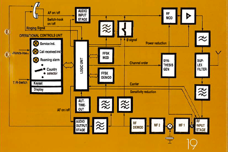
Figur 2 - Block diagram of mobile phone units,
"NMT 450 Technical Overview" promotional material ca. 1980
Note the
“Ø” signal; this is a continuous tone transmitted by the base station which is
relayed through the phone unit and measured in the base station. This signal is
used to measure the signal quality of the link and during handover. A compander/expander could also be used to improve dynamic
range if supported by the phone and base station, the latest revision of the
NMT 450 specification also allowed for a voice scrambler over the air.
Several
manufacturers made NMT 450 equipment including:
·
Ericsson
(notably the Hotline series)
·
Nokia
·
Mobira
·
Mitsubishi
(branded as Panasonic)
o
I
have one of these models, it’s next on the list for redesign when the base
station is done
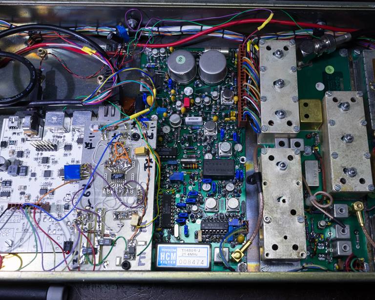
The base
station equipment I have would have been put in a rack with 8-16 sets of
receivers and transmitter + support equipment. The layout probably looked a lot
like this:
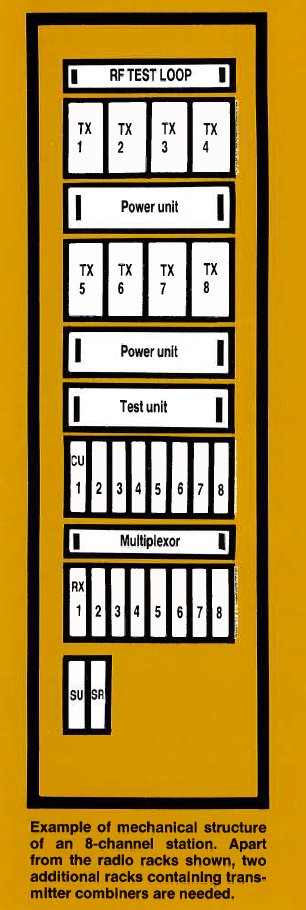
Figur 3 - Typical base station rack
The layout
would use a band pass filter+splitter to run up to 8
receivers off the same receiver antenna, and a power combiner+filter
to combine the transmitters. I’m not sure if single antenna systems were used
or if multiple antennas were used here. It is likely these were either cavity
or helical filters. Helical filters and dielectric resonator filters were
common in the mobile unit combiners, which required fairly good performance to
achieve the required sensitivity, these filters are worth salvaging as they can
often be retuned to 433 MHz.
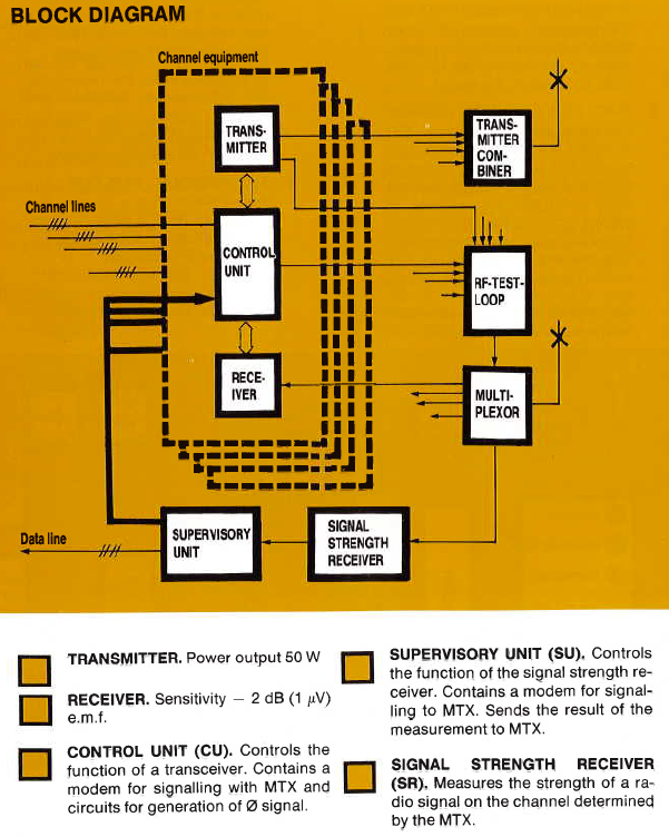
The
following figure in Ericsson Review suggests single antenna systems were used.
Note also the power measurement receiver. Not shown below is the test generator
system included in each rack to test the RF signal path.
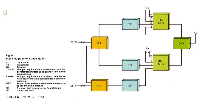
Figur 4 - Base Station Block Diagram
An article
in Ericsson Review in 1980 had a picture of a typical base station setup; I
believe this is an earlier model of my units due to some differences in how the
front panels look (notably, there’s no large BCD channel selector). My units
are all from around 1986.
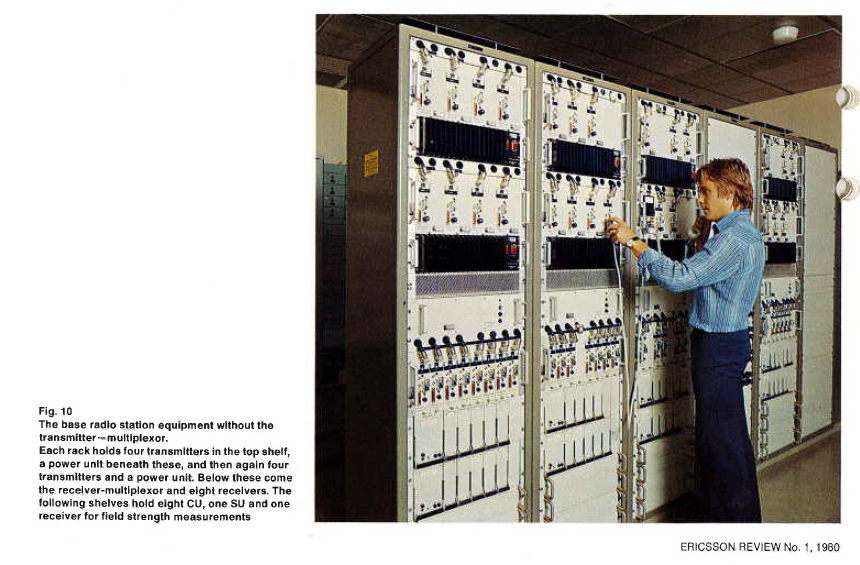
Figur 5 - Early NMT Base Station, 80s fashion
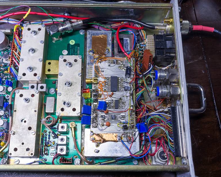
The 8801A
receiver is very similar to the F955 receiver, so a lot of the technical
documentation can be referenced: http://www.jancorver.org/en/ombouw/ericsson/f955/
The main
manual is in Dutch, but it’s still somewhat understandable due to the excellent
diagrams drawn by PA0IB.
The
receiver consists of a couple of boards:
·
1st
converter
·
Local
Oscillator
·
2nd
converter + discriminator and power
·
Remote
control board
·
Some
kind of other board
·
Various
front panel components
The boards
basically follow a block diagram of a receiver with fairly standard
interconnects, which made understanding its operation pretty easy.
The
original sensitivity specification for the receiver was the following:
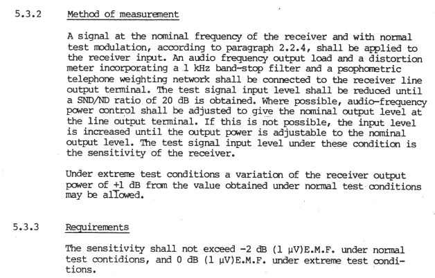
This was to
be done with a signal 10 MHz away at 80dBµV applied to the input, simulating an
active transmitter system. Note that the sensitivity is for 20 dB S/N at -110 dBm, while most amateur radios use 12 dB S/N. The
difference in effective sensitivity is e.g. -108 dBm
for 20 dB SINAD and -120 dBm for 12 dB. The squelch
opening level was also to be set to this -2dBµV level, with 2dB hysteresis.
In practice
the sensitivity of the system is largely limited by the attenuation and stop
band of the first band pass section and first preamp. Achieving better
performance than this with the requirement for very strong interfering signals
is still challenging.
Due to the
system design, adjacent channel rejection was also an important characteristic,
with a requirement being minimum 75 dB rejection of adjacent channels.
The 1st
converter consists of helical band pass filters which can be tuned, a preamp, a
second filter pack, a MCL RAY-1 mixer, and the IF output. The LO input is 10 dBm nominal and in this design seems to be multiplied by
two on this board (block diagram for the F955 version shows only one doubler but this version has two of them in series).
I decided
to replace the original preamp with a PSA4-5043+ mounted as a little sub-board
on the bottom layer. This improved the performance a fair bit, though I did
have to re-tune the filters after the replacement.
The coils
inside the filters had to be extended about ¼ turn to let me tune them; I know
some other modifiers simply added a new tapped hole next to the original tuning
screws to offset them that way.
I don’t know what the point is in using
set-screws for tuning here; the only difference compared to standard socket
head screws is that the set screw uses a less common 1.5mm hex key and if you
screw it down too far the set screw falls into the chamber.
One nice thing about DIN912 style screws is
that the head diameter is the same as the nominal size of the nut of the same
size so you can get a ring spanner over the head for tightening the nut in an
application like this.
The board
runs off a single 8V supply. I believe the other pins may be an LO power detector,
but I haven’t looked into this yet.
The original design included a large
number of power measurement and similar test points to aid in troubleshooting.
Most likely an automatic or semi-automatic assembly tester was used to simplify
testing.
There’s no
test point for tuning, but one way of tuning this circuitry is with a noise
source + marker generator on the input, the 21.4 MHz IF is not filtered on this
board so the full bandwidth can be tuned that way. Another way is to use an RF
probe on the mixer input with a tracking generator on the input. Frequency
range after retuning is approx. 432-436 MHz.
With a tracking generator and a mixer it would
be possible to mix the tracking output with the same frequency as the receiver
LO to move the tracking output to the nominal input frequency.
The coax
stub near the mixer should probably be extended slightly, but I haven’t done
anything about that. I believe it’s tuned to the image frequency of the mixer.
The doublers and LO BPF can can be
tuned for maximum signal output, but as long as the LO is sufficiently strong
there are diminishing returns wrt. how
finely these need to be tuned. I recommend lubing the slug tuned transformers
in the corner with PTFE spray before any tuning is attempted since they tend to
crack otherwise.
I modified
my converter by replacing the first LNA with a PSA4-5403+ board cut out of
single sided PCB stock and wired to the appropriate filters, a 7805 regulator
can easily be installed on the bottom layer as well. Keep in mind the bottom layer
height clearance is only about 5mm in this chassis so keep components low. I
don’t know if this improved anything, but the filters had to be retuned after doing this.
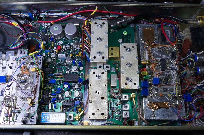
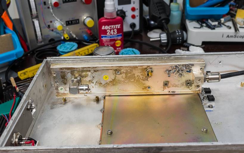
Figur 6 - 1st converter before modification
Figur 7 - Block diagram of the 8801A receiver 1st
converter
The LO
generates 6.25 kHz spaced frequencies which are multiplied up by 4 in the 1st
converter board and used as a low side LO for the mixer with a 21.4 MHz IF.
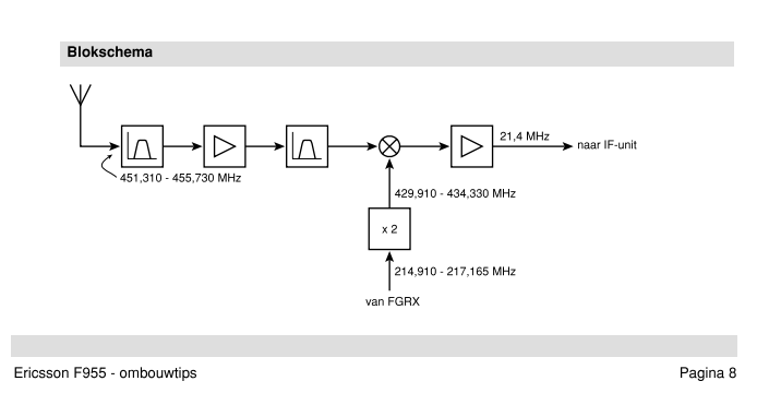
The Dutch
F955 version is fairly different since channel spacings
were different which required a lot of additional circuitry. This version is
fairly simple.
A 4 MHz
reference is used instead of 4.225 MHz. A fixed 104
MHz reference is made using a multiplier off the 4 MHz.
The VCO is mixed with this signal and amplified and fed into the PLL IC which
is made by Harris. Control input to the PLL was 3 BCD digits that were summed
with a binary input that would typically be fixed. This type of interface is
ideally suited for connection to BCD switches.
I broke the
PLL IC in my unit when I powered it off a wall wart supply with no grounding
and touched the grounded soldering iron to a pin, basically an EOS failure. As
such I had to hack up a board with a new PLL that sits on top of the original
circuitry, which is shown in the picture below.
The rest of
the circuitry was maintained.
To get the
synth working you might need to consider the wiring of the BCD switch; the
switch goes all the way back to the remote control board since this board can
remotely override the channel selection. It’s not too hard to match colours to get the BCD switch wired into the PLL directly
if you want to remove the remote board. I have no info on how that board works
and never made any attempt to reverse engineer it.
The
original LO ran at around 106-108 MHz, the new frequency range is 102.65-103.65
MHz. Because of the mixer at 104 MHz that changed the
sideband and effectively the VCO tuning polarity which is worth noting if you
intend to re-tune this. The PLL polarity can be set by changing one of the pins
on the PLL IC.
Adding some
capacitors to ground on the bottom layer was enough to re-tune the VCO to the
lower frequency. Since the control IC is socketed it’s not too tricky to remove
it and manually tune the VCO.
To re-tune
the synth for a different channel range all that is needed is to change the
binary digit inputs to give the correct N divider value at the lowest channel
number you need. Keep in mind the channel raster is 6.25 kHz at the PLL since
the LO is later multiplied by 4.
Example:
Assume lowest frequency of interest:
432.000 MHz
LO Frequency = 432 – 21.4 (known IF
frequency) = 410.6
VCO frequency = LO frequency/4 =
102.650 MHz
Here’s a complication: we have a
mixer in the feedback path, see block diagram from Ericsson below
The fixed stable oscillator is 26x
reference voltage (multiply by 2 then 11 in the can to the upper left), 104 MHz
PLL input frequency is 104 – 102.650
= 1.350 MHz
Let’s check our other end to make
sure we don’t hit the mixer:
LO_1 = 436 – 21.4 / 4 = 103.65
PLL frequency = 104-103.65 = 350 kHz
We know the reference frequency is
divided to 6.25 kHz (infer from system design, or power up and measure
frequency at lock detect/PFD output)
N_0 -> 1.350 MHz
/ 6.25 kHz = 216
Other end:
N_1 -> 0.350 MHz / 6.25 kHz = 56
Whoops, since we moved from the
higher sideband to the lower sideband of the mixer, our channel selection is
backwards.
Since the binary N value is summed with the BCD value then either you
can hope the PLL has a subtract mode, or live with the channels going the wrong
way and program the binary N to 56.
I suggest
making a spreadsheet to keep track of the channel -> frequency correlation
if you go this route. No correction is really needed for the loop filters since
the gain is likely to be about the same.
The Dutch
version didn’t have this problem since their fixed oscillator was set to a
higher value, and their LOs were all on the lower sideband to begin with.
Also note
that almost the same layout is used in the transmitter except there’s a second
set of varactors on the PLL.
The Toyocom 4 MHz VCXO is worth salvaging even if the board is
scrapped.
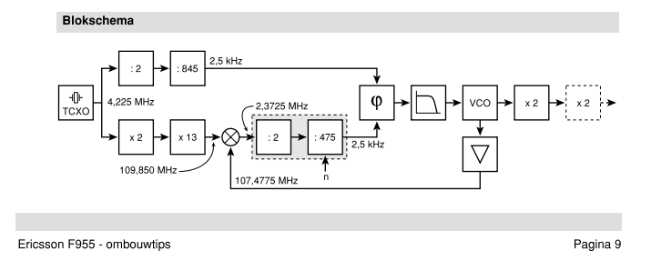
Figur 8 - LO block diagram, Dutch F955 version
Ericsson
Review also had a block diagram in their NMT 450 launch article showing a very
similar design to the production version. There are advantages to downmixing the frequency instead of pure division since the
effective N divider is lower, it also allows the use of slower processes for
the digital dividers and PFD. Mixers suitable for this application are fairly
easy to implement using discrete RF transistors, while 100 MHz capable CMOS processes
were pretty far away in 1980.
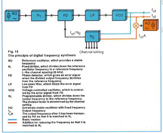
Figur 9 - Ericsson Review Block Diagram showing a
similar synth design
The second
converter has a Toyocom HCM filter with matching
components, this is an absolutely fantastic filter and well worth the effort to
desolder even if you are throwing out the board.
Ericsson also used this type of filter in their mobile units.
It is
likely this grade of filter was chosen almost entirely due to the strict
adjacent channel rejection requirements.
The metal
cans near the top are shielded audio transformers, bandwidth is quite good and
these should also be recovered before the board is discarded.
There’s no
schematic available for this board (dutch
version is somewhat different), but the SL6601 VCO based discriminator is used
for detection at quite a low 2nd IF due to the extremely good
filter. I tapped the discriminator output directly and made a little board with
AF filtering for my use with D-Star. A DV-RPTR board can be seem on the left.
A lot of
the circuitry on the board is squelch circuitry and band pass filters for the
two AF outputs from the receiver. I believe the two outputs are for data and
voice.
Due to the
filtering applied, these signals are useless for data modes.
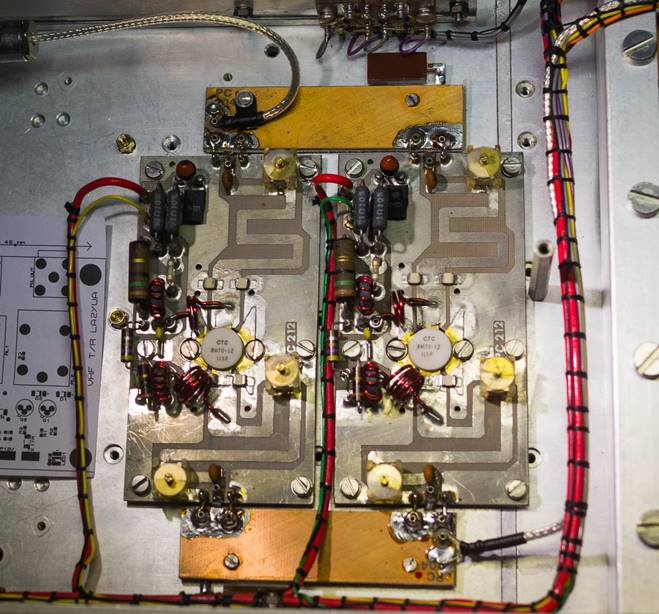
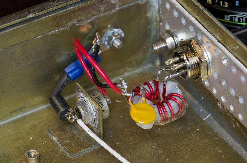
Power Amplifier System
The PA in
this unit is implemented using four sub-assemblies as well as the harmonic
filter.
Two
identical PA modules are used, along with two quadrature couplers, forming a
quadrature-coupled amplifier.
A couple of
advantages are inherent to this type of amplifier:
·
Good
input and output impedance matching guaranteed
·
High
output mismatch tolerance
·
Reduced
power dissipation in each transistor
·
Some
degree of redundancy (though less so with this design)
The entire
assembly is enclosed inside a shielded box inside the main shielded box,
presumably to avoid excessive RF leakage interfering with the control logic.
Power and monitoring signals are fed through feed-through capacitors, while the
coaxes go through notches in the enclosure.
The nominal
input power to the PAs is 10W, with approximately 50W output power. A power
detector is included on the input side, the output detector is part of the
harmonic filter.
Each PA is
a separate board, and the couplers are hybrid PCB based, Magnetic AB used this
coupler design for several other PAs too.
The PAs
operate in class C mode, running directly off a 14V power supply, separate
current shunts are included to aid in alignment and troubleshooting.
The big
advantage for a PA of this type is that any return power from the antenna
(mismatch) will primarily be dumped into R23, which is a 50 ohm 50W stud
mounted resistor. This means the PAs can tolerate more or less completely open
or shorted antennas without any issue, though obviously the total power
dissipation will be a bit higher.
According
to the schematic title this PA is designed for operation from 400-470 MHz, and
retuning is not particularly troublesome (in fact it works pretty well without
any realignment). Alignment is done by applying a fixed input power and tuning
the various trimmer capacitors on the two PAs to give the highest output power.
It’s usually better to do input matching first, then output for both of the
PAs. Checking input/output return loss is usually not required due to the
quadrature coupled design.
A plastic trimmer tool
is mandatory, and I advise against touching anything while the PA is active to
avoid RF burns.
Alternately
in a closed loop system alignment can be done by regulating a power level and
monitoring the gain control level.
The input
to the PA system is a standard BNC connector, so if the exciter portion isn’t
operational then it can also be aligned by applying an external RF signal up to
10W. The PAs are hard-wired to the power input and so as long as power+RF is applied they are active.
As
mentioned above this design is not redundant, the most likely failure is a
shorted RF transistor, since there is no separate fusing of the two PAs a
single fault will disable the transmitter.
The schematic
below is a different version of the PA, which is built as a fully integrated
assembly with both transistors, couplers, and low pass filter all on one board.
The Scandinavian version had all these as separate boards, but the general
function and implementation of the circuitry is still pretty similar.
Figur 10 - UHF Power Amplifier, complete system (F955
variant)
One of my
units had a broken output termination resistor (split in half during transport,
most likely). Keep in mind both the transistors and resistors contain beryllium
oxide if this happens.
I replaced
the broken unit with an Anaren G150N50W4B flange
mount 150W resistor instead; after removing the old resistor (held in with a
nut from the heat sink side), two new holes were drilled and tapped and the new
resistor screwed in. A piece of copper tape was cut to make a good and slightly
flexible connection to the coupler output.
The Anaren resistor is highly affordable and available as of
2017 (check eBay, a number of Chinese sellers have used ones in stock). Keep
mind that that model resistor should be installed with the flange solidly
grounded to the chassis, I decided not to use any heat sinking compound for
this reason.
Figur 11 - Placeholder PA image (VHF 100W variant
shown)
These PAs
could be suitable for linear operation if paired with a suitable bias regulator
(in class C the base bias is supplied by the RF itself, making it highly non linear).
Harmonic Filter/Output
Coupler
The
harmonic filter/output coupler is a large PCB based filter assembly with a
couple of couplers built in to provide some feedback.
The main
PCB is sandwiched between two aluminium oxide plates,
which are then covered by two silver plated copper outer plates providing the
ground plane, a U-profile covers the ends.
With this
filter the main PAs are able to produce around 50W of quite pure RF. The
filters have a notch starting around 800 MHz, with good attenuation up to
approximately 2 GHz.
The coupler
portion includes a -37dB port routed to an SMB connector and further to a front
panel BNC connector for testing, and two 3-port couplers which together
implement a 4 port coupler providing forward and reverse power. A small PCB is
mounted on the filter assembly which contains rectifier diodes.
It can be
seen below that the primary circuit topology is a notch, rather than a pure low
pass.
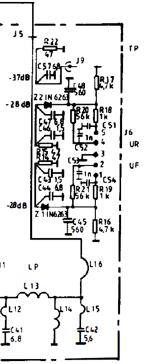
Figur 12 - Harmonic Filter, approximate schematic
Figur 13 - Harmonic Filter with rectifier board removed
The picture
below is from the TU8062 UHF power amplifier (likely used for manual UHF
telephony), I believe it’s similar to the design of the NMT variant. The
component values mounted on the coupler outputs are a match for my version.
Figur 14 - Harmonic Filter, UHF variant
Since I’m
replacing almost all of the circuitry in the receiver I decided it should be
rebadged.
Planned
features:
·
High
sensitivity - -110 dBm for 12 dB SINAD (CCITT filter
in) or better
·
“Stepless” receiver to support newer channel spacings
·
Frequency
range: 432-435 guaranteed (Norwegian 70cm allocation – space band not a
priority)
·
High
dynamic range power monitor
·
Discriminator
output for noise squelch
o
Analog
noise squelch if possible for better performance
·
Bandpass
filtered squelched AF output
·
Expander
supported
·
CTCSS
squelch with phase reverse support
·
DTMF
decode
·
5-tone
decode (for 1750 support; somewhat obsolete but cheap to add)
·
Fully
differential I/O
·
CAN
bus control interface
o
Standalone
operation with matching transmitter, or remote control.
I/O:
·
Test
Connector for alignment
·
RF
input, 50 ohm
·
LO
reference output for frequency adjustment
·
10
MHz reference input for automatic frequency control
·
2xCAN+audio
ports for daisy chaining
·
GX12
power inlet, 12-14V DC at 1A with reverse protection.
Below: the
8801A with the mk. 2 discriminator board undergoing testing. The VCO board can
be seen on the left, but the LO is generated externally in this picture since
the motherboard was not ready at that time.
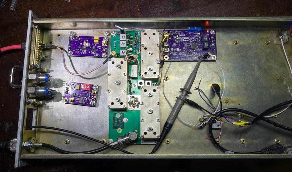
Figur 15 - LA2YUA 8801A Work In Progress (2017,
colorized)
The
following boards have been custom designed for this project:
·
Discriminator
·
Local
oscillator pack
o
VCO
daughterboard, Vackar based from 102-104 MHz
o
VCO
motherboard with phase detector
o
Local
Oscillator Interface board
§ Provides UART interface to the LO
system, implements the “stepless” PLL reference
tuning system with optional automatic calibration
·
BCD
thumbwheel I2C interface
This board
accepts a 21.4 MHz IF input on an SMB connector, this signal is filtered,
amplified, converted to 455 kHz and detected in an LC tank discriminator.
Mechanically the board takes up around 1/3 of the area of the original
discriminator and fits the same mounting holes.
Interface
is 8V power supply, unfiltered AF output (~200mV RMS at 5 kHz deviation), power
detector output (AD8307 direct output), DC coupled quadrature detector output,
and a tuning input for the LC tank.
The
original V1 version used a PLL detector, but this caused problems with
interfacing to the MC3374 IC and so was redone with some additional features to
improve sensitivity.
Sensitivity
for 12 dB SINAD (with CCITT filter since it’s unfiltered): -110 dBm or worse. Performance is better when shielded inside
the case of the receiver.
The input
is approximately 50 ohm, the input is then matched into a 15 kHz wide crystal
filter. The output is amplified by a BF996 FET amplifier and further amplified
by a BFG94 amplifier. The amp output is coupled to an AD8307, and proceeds to a
match into a MC3374 IF subsystem IC. I picked up a bag of 250 pcs. MC3374s for
very little money, so using this IC made sense.
I could
have reused the Toyocom filter for this board, but
since I couldn’t find any more of them I decided to use some more commonly
available filters since the board will be useful for other projects as well.
The specific filters were designed for Uniden marine radios, I picked up around
200 of these for a good price.
The MC3374
includes a crystal oscillator (20.945 MHz), mixer, two
IF amplifier stages with two ceramic filters, and a quadrature discriminator
with a discrete LC tank circuit which can be tuned using a varactor.
The original recommended tank part is nearly impossible to find, so a discrete
solution seemed like the best choice. Ceramic discriminators are specifically
not supported in this IC.
The
discriminator output is AC coupled and amplified then output, the output is
also low pass filtered and amplified to allow external circuitry to detect the
DC offset of the tank. The tank can then be automatically temperature
compensated using an external feedback loop. An on-board trimmer sets the
correct LC tank tuning when no external circuitry is connected to simplify
testing.
The power
detector has a noise floor of around -70 dBm at the
input due to a minor design error which means the 2nd LO is coupled
back to the detector. This issue is minor enough that I’m not planning on respinning the board. For a potential future revision the
detector should be coupled directly after the filters through a separate FET
amplifier.
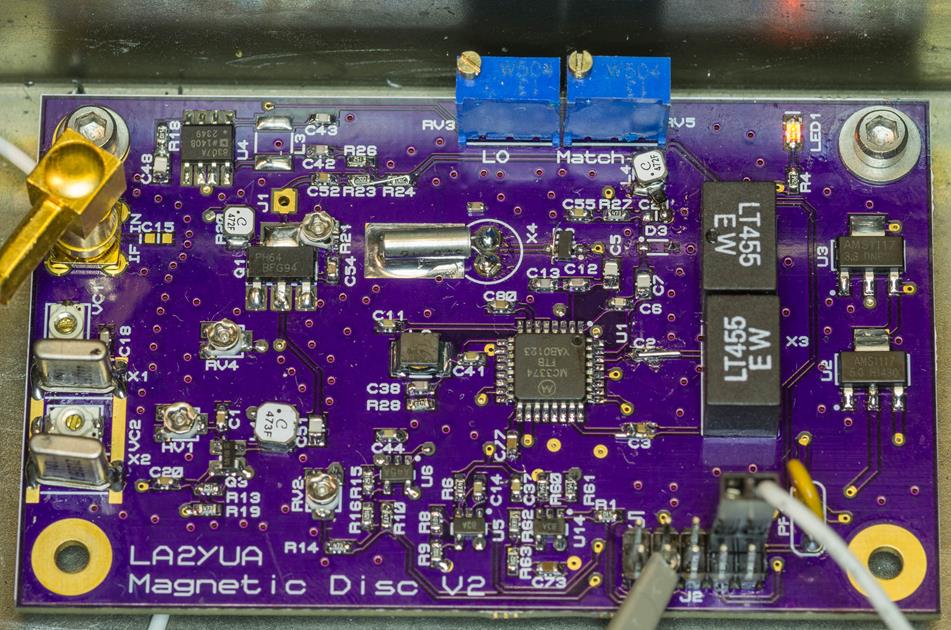
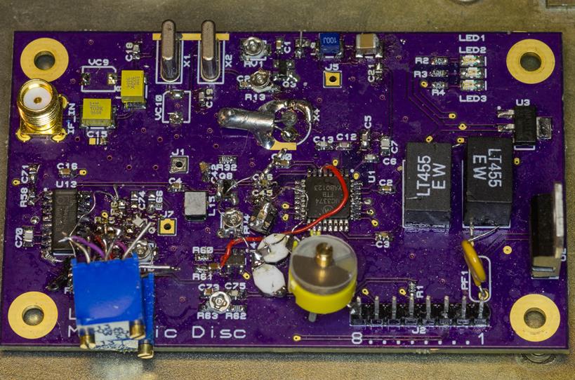
Figur 16 - Discriminator, version 2
Vackar
oscillator tunable from 102-104 MHz minimum. Output power port 1: +10 dBm +-2dB. Output power port 2: 0 dBm
to PLL. 4 layer board with continuous ground and power plane.
Uses a
BFG580 oscillator transistor with regulated collector current (6mA DC, with LF
feedback for lower noise), and a BFG135 output buffer. I believe a low noise
transistor is advantageous for the oscillating transistor, the BFG135 is not
low noise but this is not as critical.
The design
is somewhat sensitive to output loading, but when used in a constant-load
system this isn’t a big problem. The same board can be tuned for 89-91 MHz for
use in the transmitter with only a single capacitor change, the Vackar design is very flexible and convenient to use for
this reason. The circuitry runs entirely off a 5V locally regulated supply, so
PSU noise is not a big problem.
The main
inductor is a KOA SPEER 100nH 1210 inductor, this inductor has proven to be
highly stable so I recommend using this. The 1µH inductor on the collector is
mainly used to improve voltage gain in the amplifier.
The
stability of the VCO is quite good once warmed up, the collector current
regulation also improves low frequency phase noise.
Power
supply: 6-10V (8V nominal). Designed to mate with a PLL motherboard to lock the
VCO to a specific frequency.
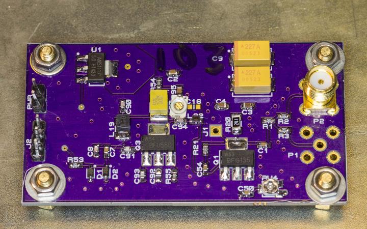
Figur 17 - VCO board assembled
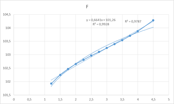
Figur 18 - RX VCO tuning characteristics
This board
has a thermally regulated VCXO reference oscillator (77.76 MHz nominal; tuned to
77.75 MHz), a MC145170-2 PLL IC, and a loop filter. The board fits two of the
original holes for the LO and can be installed quite easily. This also fits the
transmitter hole pattern.
The nominal
reference frequency is 6.25 kHz providing a 25 kHz channel raster when the LO
is multiplied in the 1st converter. Loop filter bandwidth is 1 kHz
with an integrator type filter.
Connections
are made to allow the VCO daughterboard to plug into the top of the unit, this
had a couple of advantages since the VCO could be 4 layer while this board is 2
layer, saving money. In addition the VCO itself could be built separately to
reduce risk and it can be swapped out quite easily if a better design is called
for. Board footprint is also reduced while keeping the design quite open and
easy to work on.
The I/O is
a 6 pin DIL header with SPI and Lock Detect, a 2 pin header with 8V input, and
a 3 pin header for the VCO tuning voltage.
The mating
interface is a 2 pin female header with power, a 3 pin header with the tuning
voltage, and a MCX connector for the RF feedback. MCX connectors are well
suited here since they’re the same height as standard 0.1” headers when mated.
77.76 MHz
may seem like an odd choice for this VCXO, but since I picked up around 750 of
these MC349 (now Vectron) VCXOs on eBay I had to use
them for something. They also have very fast CMOS outputs, good tuning range,
good stability, and linearity. The tuning range and bandwidth is good enough
that a low distortion modulator can be implemented using these as well.
A
LM35+TIP32 transistor circuit is used to regulate the VCXO case temperature to
around 50*C. The sensor and transistor are simply glued to the case of the VCXO
using Loctite 480 super glue. A higher temperature could have been used but
this would have required a more expensive glue to tolerate the temperature.
This board
controls the VCO motherboard, it accepts a specific frequency to generate over
UART and calculates the appropriate PLL settings and transfers them over SPI.
Lock detect is also monitored for BIT feedback.
To hit
frequencies between the channel raster, a trim-DAC is used to tune the VCXO on
the VCO motherboard. This can offset the reference frequency to allow more or
less stepless tuning. For a receiver this is not very
critical, but the same board stack is used on the transmitter where stepless tuning is more relevant.
To know
what the “correct” voltage to set is, the unit accepts a control voltage from a
front panel trimmer which is used as the nominal control voltage to start from.
In addition, when a 10 MHz reference is available, a PLL is used to slowly lock
the VCXO to the external frequency. The control voltage is then measured with
an ADC and the locked voltage is stored in memory. This PLL is only activated
periodically as a calibration and is not used continuously. Sensing circuitry
is included to detect the frequency present at the reference input, to detect
when automatic calibration is available.
This board
also outputs a copy of the VCXO frequency which is routed to a front panel test
connector that can be used when manually adjusting the frequency. As the VCXO
is heated, the calibration interval is fairly long.
A possible
application of this stepless design for standard FM
is to automatically center the receiver on incoming signals to improve AF
performance. This would involve feedback from the AF processor board looking at
the discriminator DC offset.
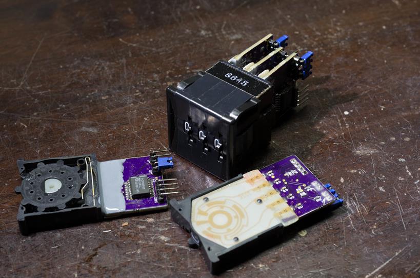
Originally
the channel selector was a 3-digit thumb wheel connected to the control
circuitry and LO board. In order to reduce the amount of wiring some boards
were made that could sit on the back of the thumb wheels and provide an I2C
interface.
Each unit
has two BCD digits from 0-9 and one decimal digit limited to 9-1. The limit
pins were removed to allow all digits to read 0-9.
The actual
board is a PCF8574 I2C I/O expander connected to the ABCD lines, a LUT is used
on the host MCU to convert this to digits. On the decimal boards this interface
wouldn’t work, so an inverted input 10-4 priority encoder is used to convert
the decimal lines to the same BCD format as the normal BCD lines.
As can be
seen in the picture below, the boards are fairly small, and are soldered +
epoxied to the frame of each digit assembly for mechanical support (Hysol 3450 was used, but DP490 would also be a good choice).
Jumpers set the I2C address of each digit.
This board
will have AF processing and squelching circuitry.
The AKM AK2345
radio baseband IC is used for AF band-pass filtering and CTCSS decoding, this
IC has switched capacitor filtering which is significantly better and more
compact than using discrete filters for the same job.
A DTMF
decoder is used to detect DTMF inputs which are reported digitally for
processing by the receiver controller.
A
comparator + frequency counter in the MCU can detect slow FSK signals directly,
e.g. 5-tone or 1750 tones.
A SA571
expander IC is used to implement an analog noise squelch (signal is attenuated
proportionally to the noise level, this reduces the noise burst at the end of
transmissions). Analog noise squelch is a fairly rare feature, I have only seen
it used in my FDK Multi-2700 from the late 70s.
The second
half of the IC is used to implement an N2 expander which can be switched in to
the signal path. This is especially useful for backhaul applications with
linked repeaters since the SNR of the link is improved significantly.
A copy of
the raw discriminator output is scaled and output directly with no further
processing for connection to data modems.
The power
measurement output and discriminator DC offset signals from the discriminator
are digitized on this board.
This board
interfaces the BCD switches, trimmers, test connector and LEDs.
This board
has filtering, line drivers, and interfacing to the RJ45 connectors on the back
of the unit.
STM32F103
32-bit Cortex-M3 MCU, CAN
A new 1st
converter could be made to utilize relatively commonly available ISM band SAW
filters for better selectivity in duplex applications.
The design
would probably involve a PSA4-5043+ preamp behind a bank of selectable SAW
filters.
I currently
have a supply of 433.42, 433.92 and 434.42 MHz SAW filters which are around 800
kHz wide, these provide good attenuation outside the pass band. Combined with
the same set of filters in the transmitter exciter path a duplex system for
dual antenna setups could be implemented fairly cheaply. Some consideration
would be necessary wrt. input
protection since SAW filters typically don’t like more than 0 dBm on the input. A PIN limiter could be used for broad
band suppression after an initial LC band pass filter.
As a high
linearity mixer would be required, an LTC5510 has been on my list of good
candidates for a while.
110.51 MHz
might be used as the 1st IF instead of 21.4 as I have 40 kHz wide
crystal filters for this frequency, a second converter would then be used to
generate 21.4 MHz for the discriminator. This would simplify image rejection on
the front end, but would also complicate the design a bit. The AD831 active
mixer would be a suitable choice for the 2nd mixer due to the high
linearity and decent noise figure in this frequency range.
The LA2YUA
variant of the 8802A transmitter has the following features:
·
Operates
from a single 13.8V nominal supply
·
432-435
MHz guaranteed frequency range
·
50W
continuous output power
o
Adjustable
from 1-50W “stepless”
o
Capable
of operation into open or shorted antennas with no derating due to the
quadrature coupled output
·
SWR
measurement for error reporting
·
-60dBc
or better harmonic performance
·
Sub-band
filtering on exciter to reduce in-band noise for duplex systems
·
Arbitrary
frequency step
·
High
linearity modulator
o
+-1.25,
2.5 and 5 kHz deviation supported
·
Direct
modulator input and filtered AF input selectable
o
Differential
I/O only
o
AF
bandwidth 300-3000 Hz
·
DTMF
encoder
·
Subtone encoder with reserve burst
·
DDS
tone encoder
o
E.g.
2/5-tone
o
Adjustable
frequency and phase, can be used for simple FSK
·
Selectable
AF N2 compander
A Vectron VX-500 type VCXO is used as the modulator in this
system; the VCXO operates at 77.76 MHz and can be modulated up to +-5 kHz with
low distortion. The VCXO is temperature regulated using the same solution as
the receiver LO generator for improved stability.
The full
tuning characteristics are shown below:
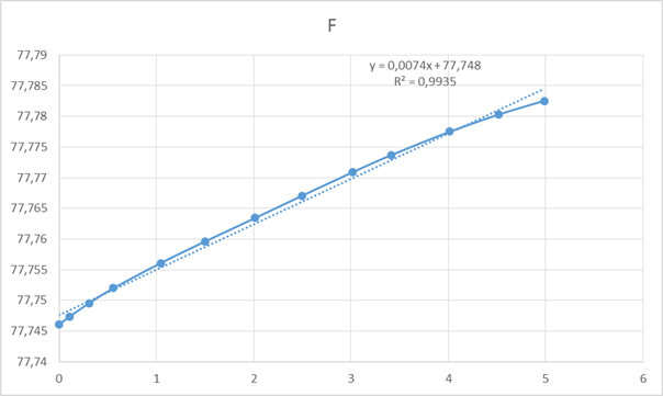
Figur 19 - MC349 VCXO tuning characteristic
The best
narrow band performance can be attained at a DC offset level of 1.5V with
0.833Vp-p voltage swing or less.
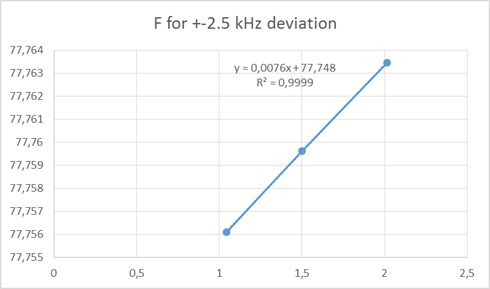
Figur 20 - 2.5 kHz deviation response
For 5kHz deviation, a slightly higher DC offset gives the best
performance at 2.125V with 1.55Vp-p signal.
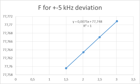
Figur 21 - 5 kHz deviation response
The center
frequency at the nominal offset is measured during assembly and programmed into
the main controller, the LO generator is offset appropriately to give the
correct output frequency.
The BPF70
sub band filter module is a sub board that can be used in both the transmitter
and receiver signal path to filter unwanted sidebands from the signal of interest.
The filter
is implemented as a daughterboard that can be installed in both the TX Exciter
and the RX 1st converter, two MCX male connectors + 6 male 0.1” pins
are the only interconnect.
The board
accepts power and two digital control signals that are decoded and selected to
various RF filters, a polyfuse protected bias-tee is
available for use with active receiver antennas on a separate pin header.
The
following filter characteristics can be achieved using the module:
·
Broad
band (420-440 MHz), “bypass” using only LC filters
·
433.30-433.54
MHz using TDK B3791 SAW filter – UHF Sub 1
·
433.55-434.30
MHz using TDK B3555 SAW filter – UHF Sub 2
·
434.25-434.75
MHz using TDK B3557 SAW filter – UHF Sub 3
The SAW
filters in use are primarily intended for ISM band remote control devices (e.g.
garage port openers), and as such have fairly low insertion losses. I
stockpiled a number of these filters from eBay sellers over a few years for
this purpose (except the B3791, which I bought off Digi-Key since it’s harder
to find second hand).
Out-of-band
attenuation in these filters varies, and to provide broad band + image
rejection the LC filter is always included in the signal path when the SAW
filters are used.
HWS408
reflective SPDT RF switches are used to select the four different
configurations, decoding is simple and implemented using 4 inverter gates, two
LEDs also show the state of the digital inputs on the board.
The input
is protected against overload using a PIN limiter to prevent damage to the SAW
filters.
<image of all filter responses>
As can be
seen, the sub 1 filter has the best broad band performance, as well as the
highest insertion loss. For a duplex repeater this frequency band would
typically be allocated to the receiver. Slightly higher performance may be
attained by using this frequency for the transmitter where the insertion loss
is compensated by the power regulation circuitry.
Due to the spurious characteristic
of the filters, transmit and receive frequencies should always be carefully
chosen after consulting the relevant measurements.
When these
filters are used in both the exciter and receiver, sufficient isolation is
attained that a dual-antenna full duplex system can be set up provided the
duplex spacing is set up such that the transmit and receive frequencies each
use one of the SAW filters (the TX chain filtering is used to reduce the amount
of phase noise present at the receiver frequency). The RF power detector built
into the discriminator can be used to verify the achieved isolation.
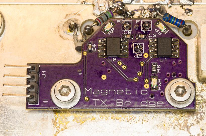
<image of board>
The output
harmonic filter includes a 4-port power detector available on a couple of pins.
Originally a small PCB with rectifier diodes were used here. Since I wanted to
regulate power across a wider dynamic range, I replaced this board with a new
board based on two AD8307 detectors.
My initial plan was to install SMB connectors
and put the detector on one of the other PCBs, but this was dropped due to
space constraints + the fact that soldering anything to the harmonic filter is
nearly impossible due to the enormous thermal mass.
The mounting screws for the old board were also
right there, and OSHPark pricing meant that it was
actually cheaper to build a couple of these boards than it would be to buy the connectors+coax to mount the detectors elsewhere.
The AD8307
was chosen specifically because it has a very large dynamic range and its
extremely low cost (80 dB useful dynamic range at 430 MHz). Note that 2-port
power detector exist, these are useful since they will be matched; the AD8307s
are not matched and have to be software compensated for primarily offset
related errors.
This
solution allows power regulation down to below 1mW output power, while still
providing the required accuracy at up to 50W output power. Reverse power
measurement is sufficiently good that a reasonable SWR estimate can be made,
and power may be de-rated based on this reading if required.
Two LEDs on
the board illuminate proportionally to power starting at around 10dBm input
power, they are mostly there to look cool though.
At low
detected power levels a lot of ambient noise couples in, and a low pass filter
must be used. A lower bound for valid power readings should also be set
experimentally to avoid regulating off poor quality sensor data. For a well
matched antenna the return power will be well below the forward power and will
have more noise; thus at low power levels the reverse power measurement should
be ignored for regulation purposes. It is more common to regulate to an absolute
return power level rather than the SWR reading in any case.
The actual
coupler provides 40 dB isolation and seems to read down to around 20 dB return
loss.
Figur 22 - Transmit Power Detector
A couple of
other changes were made to the chassis and related components.
All slotted
screws were replaced with allen
or Torx head screws, A2 stainless or better. Several
of the original screws had rusted due to improper storage in ham warehouses
(basements and garages).
All units
in this system used a 37 pin female D-Sub connector on the front panel for
testing of the system. This connector was damaged on several units and was
replaced with a new Amphenol cadmium plated connector.
The pinout
of the new connector was designed to interface to a Wavetek/Schlumberger
4015 test set, accordingly there are discrete digital inputs and keying/squelch
control inputs to support use of the built in testing in the Stabilock. In this mode the Stabilock
can remote control the channel selection of the unit, and several analog
signals are routed out to BNC connectors that can be plugged in to monitor
various AF signals and excite the modulator for transmitter testing.
The pinout
was also designed to be somewhat compatible between transmitter and receiver to
allow the use of a single test adapter cable.
The
original control and power inlet used an Amphenol backplane connector, the
cutout for this connector was plugged with a piece of aluminium
(various sizes depending on availability) and holes drilled for GX12 (receiver)
and GX16 (transmitter) connectors. A 100µH common mode choke is used, along
with a 500mA polyfuse with a 1N5408 reverse
protection diode on the input. The original 16V Zener diode protection was not
retained for the receiver but proved impossible to remove in the transmitters
(due to the thread locking and the soft metal of the diode body) and so they
were left in place.
A BNC
connector was also installed to support 10 MHz input locking of the system;
there wasn’t any room on the front panel otherwise I’d have put it there.
The
original feed-through diode seems to be welded or soldered to the chassis and
so was not removed.
On the
transmitters a 6x30mm 10A fuse holder was installed on the front panel since
upstream fusing can’t be guaranteed in this ad-hoc setup. The same location was
used in the TU 8131A 100W VHF amplifiers used for OLT telephony so it provides
a nice continuity.
Figur 23 - GX12 power input
A piece of
conductive gasket material was installed near the front and along the rear lip
of the steel top cover, this had a significant positive effect on the noise
floor of the unit during initial testing. Approximately 10 dB improvement in the
noise floor of the system was observed when these gaskets were installed.
The front
gasket is easy to cut and compresses, it is held in place with Loctite 401 at
regular intervals; this glue doesn’t bond well but due to the mechanics of this
gasket it stays in place. For the rear lip RTV silicone glue was used to allow
for more compression.
The same
gasket solution is used for the front shield in the transmitter, but the panel
design doesn’t permit easy shielding at the rear.
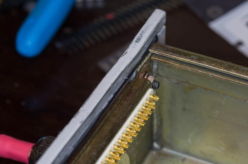
Figur 24 - Shielding for top cover
To
investigate a simple way of generating local oscillators the CDCR83 was put on
a 4 layer board and fed with frequencies from 10-150 MHz at various
multiplication settings. As usual a bag of these was found on eBay and as such
there was some incentive to find a use for them.
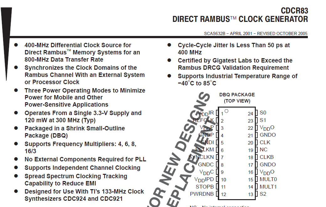
Figur 25 - CDCR83 Datasheet
The CDCR83
board:
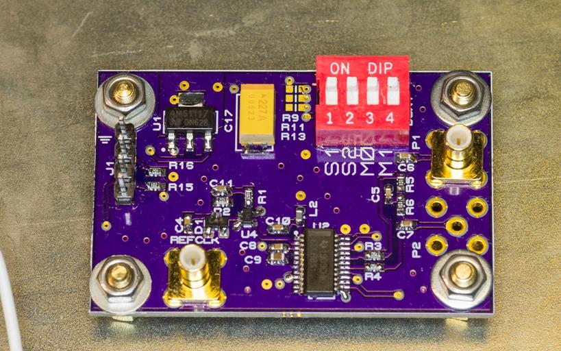
Figur 26 - CDCR83 test board
This board
runs off 5-12V and provides an I2C I/O expander interface to remote control the
IC settings including stop/power down. The DIP switch was used for initial
testing but can be overridden by I2C.
Performance
was very good considering it’s a digital clock type IC. In addition it was
found that the PLL locking range of the IC tested was actually between 40-700
MHz despite only being guaranteed for 267-400 MHz.
Note that
the additional edge-locking functionality is disabled on this board, normally
this would be used to align the clock edges of two RAMBUS clock domains. By
grounding these pins this circuitry is disabled and the phase noise performance
improves slightly.
Output
power as implemented was 0-3 dBm single ended
depending on frequency, with a very clean spectrum. It was also noted that
narrow band FM would be carried straight through (and multiplied in deviation
as expected), this is explicitly supported as the IC supports spread spectrum
clocking.
With an
appropriate balun the output power should be
increased slightly. A 1:1 50-50 ohm balun would be
best suited as the output impedance of the drivers are around 25 ohm for
approx. 50 ohm differential output impedance.
This
simplifies the generation of local oscillators for UHF systems, as a simple low
frequency VCO like the type used in this project can reliably be multiplied
with a minimum of components. The input power must be 8-10 dBm
to support proper operation, which is achievable with standard CMOS buffering
at these frequencies. The Magnetic VCO board also provides sufficient power to
drive this IC.
The low
output power is not a significant problem if the output is fed to an active
mixer as these typically run between -10 to 0 dBm LO
level. For passive mixers a higher power level is usually required and the
signals require amplification.
No project
is without some setbacks. Here are some things that didn’t work out:
The CDCE913
looks pretty good on paper, and it can generate pretty good clean signals. At
least it can when it’s doing integer multiplication.
The output
when operating in fractional mode was atrocious with spurs across the entire
frequency span of my analyzer. An attempt was made to use it with the V1
discriminator but was definitely not successful. It wasn’t even possible to get
any audio out of the system when this LO was in use.
The board
did serve as the origin of the idea of using offset tuning on the reference to
hit all frequencies; the 913 is fractional N but still can’t hit every single
frequency. Two versions were made, the original used a 14.4 MHz sine wave clock
and a 2 layer layout. The next version kicked things up a notch by using a
77.76 MHz CMOS output clock with a 4 layer board and an output buffer IC. Both versions
performed about as well (not well.)
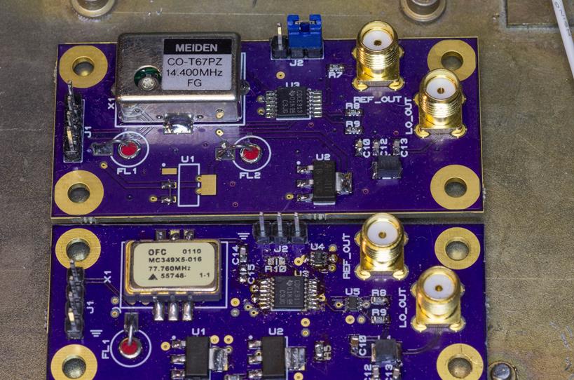
Figur 27 - Two terrible LO boards
After the
failure of these boards the current VCO board was quickly put together using
schematic bits from a planned cheap and simple VHF radio that some of the radio
parts in this system were purchased for.
The
original discriminator used a 4046 PLL (later a 9046) and the internal RC
oscillator. The concept is simple and similar to the current design except instead
of a tank circuit, the tank output is buffered, amplified, and fed into the
4046 signal input.
The 4046
keeps its own VCO in tune with the input frequency, due to the good linearity
of the VCO the output is a good representation of the FM signal.
This is all
well and good but it didn’t work well, stabilizing the loop was tricky, and
getting sufficient bandwidth for low distortion across the frequency range was
also tricky. The design of the 3374 tank output also meant there was always a
signal present on the LC output. This degraded the sensitivity significantly
since the signal had to be tapped off before the 2nd ifs 2nd
IF amplifier instead of at the end of the chain. The PLL circuitry can be seen
on the left side of the board.
After two
days of working on this board, I decided enough was enough and hacked in an LC
tank circuit (bottom middle) and tapped off the normal discriminator out on the
MC3374. I immediately achieved slightly better performance with this approach
than with the very best PLL tuning. Additional work got the distortion figures
down to very good levels.
I later
realized that the SL6601 discriminator actually just locks onto the average
center frequency of the input which locks at 90 degrees to the input; these
signals are then detected in a standard quadrature detector instead of actually
tracking the VCO along the signal.
Figur 28
- Discriminator, 1st prototype