
Precision UTC Clock Using Fiber Optic Distribution
Some viewers may have noted some 7-segment clocks in the background of some pictures in prior entries. I decided to update this system for the 2020 holiday season, and built 10 new clocks to replace 3 old ones.
Table of Contents
A Picture
There are more pictures below, but there's a big pile of text first.
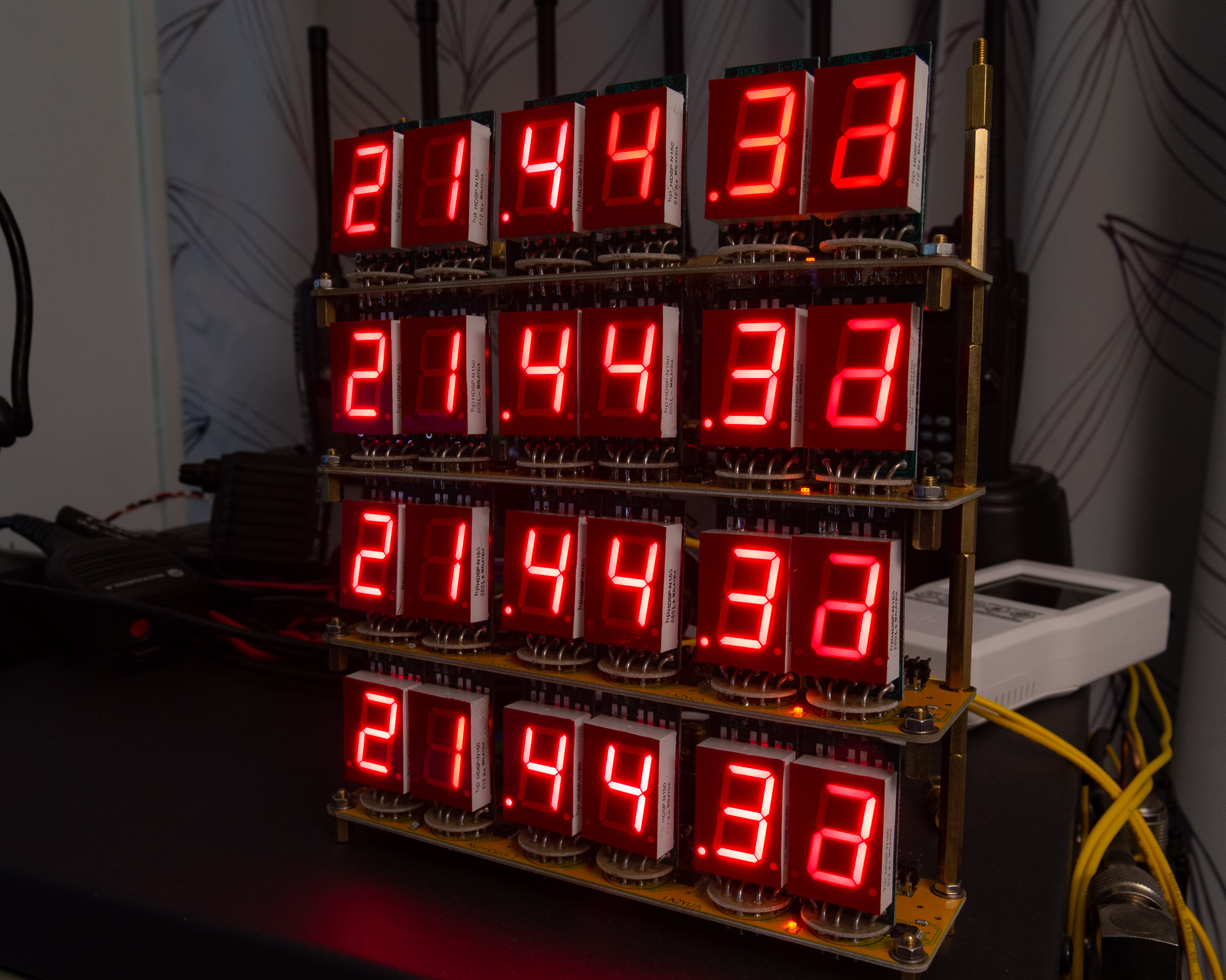
Note that the uneven brightness in some digits is made significantly more visible by the camera.
Background - The Original NumiClock
My previous clock system was fed by a set of Lucent RFTG-u modules using the standard 1PPS/RS-422 output port. I also built a distribution amplifier for these signals which added a 12 V bias power line to the 9 pin D-Sub.
This system was in operation from late 2015-2020 and worked fairly well. The primary issue was power distribution over the standard Cat 6 network cable I used. In the end using a local power supply was a far better choice.
However, using a local power supply meant adding a galvanic connection between multiple outlets, and in some cases this caused significant RFI issues due to common noise noise from the power supply. Basically it formed a big loop antenna.
The clocks used salvaged 7-segment modules as the displays, these are built to sit in a socket for an original Numitron display tube (hence the name NumiClock). I decided to keep using these displays since I had enough of them left to make 10 clocks.
They had an atMega168P 8-bit AVR processor running at a blazing 20 MHz to handle receiving the 9600 baud UART data and updating the display when the 1PPS line changed. The clocks were later updated with a red contrast film to improve visibility in bright environments.
The signalling is basically: T–~300 ms: UART time code sent containing the time to display, T+0: 1 PPS changes from idle to active, display updates. This meant that the display update was the same for all the clocks, and the update time was at or very near the actual start of the UTC second instead of being random.
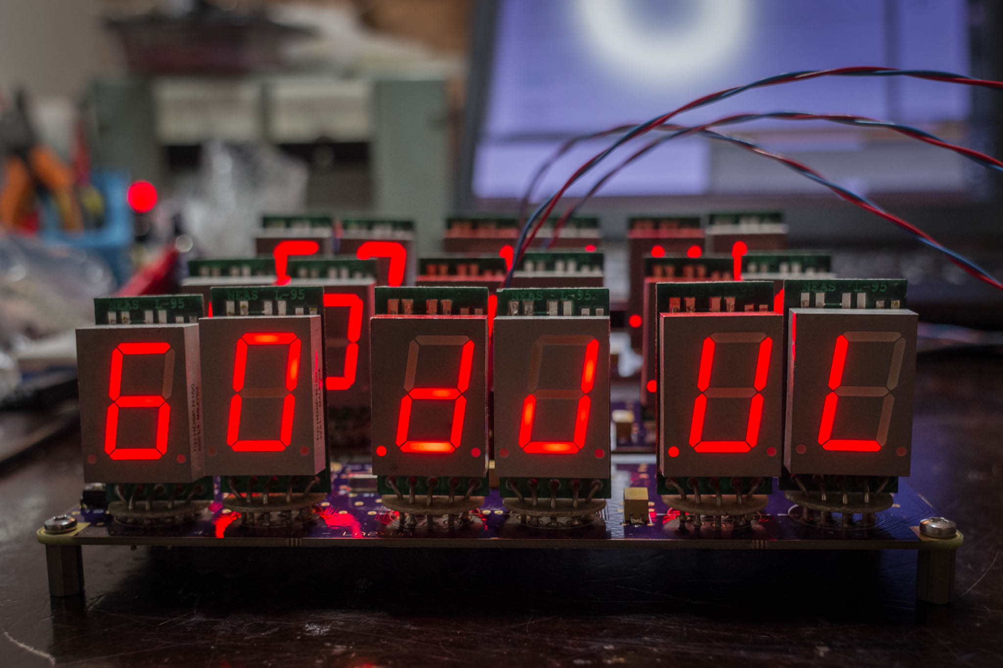
The original electronics were fairly simple, built on a 2-layer board with all linear regulators and 74HC595+ULN2003 drivers. The display modules are not compatible with PWM, so dimming is linear.
This is somewhat problematic at low intensities since the brightness between segments and displays is not matched at low currents. Unfortunately this issue remains with the new version, but if you never run the displays at low brightness it's not a problem!
System Design
There were several issues with the old clocks and the system as a whole, including those mentioned above:
- RFI issues unless powered with good power supplies and properly grounded at each end
- Old distribution amplifier was not a great design, using D-Subs was convenient but they are annoying and fiddly to use
- AVR architecture - I prefer to use STM32 based devices now
- The original Lucent RFTGs were retired in 2020 and a custom uBlox LEA-M8F based system was installed instead, so no requirement to stay with that system
- I also needed a system to distribute precision frequencies - some synergy would be nice to have and coax/network cable was not acceptable for that purpose
Having designed the HFoF fiber optic antenna, I was already familiar with and had plenty of materials for using single mode fiber to distribute signals.
This solves the RFI issue completely, and the signal can be passively distributed if a suitably powerful laser source is used. I also had a small pile of spare PIN diodes sitting around that weren't quite right for the RF systems. This would mean a one-way link to the clocks, so automatic delay compensation is not possible here.
The primary issue of using fiber optics is that unless you don't really care about price or practicality, you want to fit all you can on a single fiber. Further, it's very practical if the signal transferred is also a square wave (no analog frequency multiplexing). This is beneficial since it makes the system compatible with standard SFP or SFF modules used for digital data transmission (cheap, and easy to make active repeaters).
That square wave should also be DC balanced - this is not a hard requirement but it makes detector and modulator design much simpler since transmission losses don't affect the signal baseline.
Putting The Toothpaste In The Tube
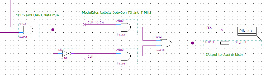
So my system needed to fit the following signals onto a fiber optic link without using any analog or RF tricks — this system is all digital except for all the analog parts: UART data, 1 PPS signal, frequency reference.
Based on some LTSpice simulations I came up with fairly simple design: The system uses straight binary unfiltered (uncensored) FSK to transmit data, the mark (high) frequency is 10 MHz, and the space frequency was originally 5 MHz but I ended up using 1 MHz to get a better signal to noise ratio. This works fine since the fiber is basically a lossless transmission medium with infinite bandwidth (for our purposes here).
The UART data idles high and is only active when sending a time code, and the 1 PPS is simply sent as a UART 0x00 byte.
To extract the frequency standard from the signal, a PLL with digital loop filter can be easily built (note: not yet built or designed). The system can use a very slow loop filter, and preferably also include a detector for the UART data to gate the phase-frequency detector (PFD) during those (highly predictable) time intervals.
The system can be coherently demodulated by frequency locking as above to the signal, and using some D-latches and XOR gates. This allows for very low jitter and low latency detection of the information signal with no analog step.
The clocks are simple devices however, and phase locking sounds hard. The clocks use a cheaper and simpler detector: the clock MCU has a programmable clock output (a few dividers + a PLL for the master clock) that can output a fairly limited but still pretty wide range of frequencies.
The FSK signal is therefore directly applied to a phase-frequency detector (at 10 MHz), the MCU generates a suitable reference clock to feed to the other input. The FSK will normally be significantly higher than this frequency, and significantly below it when the space frequency is sent.
The PFD output is filtered and converted to digital using a comparator with adjustable threshold and hysteresis.
Timing
The system as mentioned is primarily intended to display the current time (UTC or local time). It is essential that all clocks are perfectly synchronized, otherwise there wouldn't be much point in doing this whole thing.
My system timing is currently set by my uBlox LEA-M8F based timing system (the GPS feed a fairly sophisticated MCU which then outputs the timecode signal which previously emulated a Lucent RFTG).
I decided to send at T–300 ms a string framed like a Lucent RFTG signal containing some status bits, a 64 bit time_t (~Unix time UTC), and a CRC-32 of the time_t.
The UART timing is reliable to within ±1 ms due to the RTOS timing jitter in the transmitter. The 1PPS signal however is directly generated by the GPS module and has no significant jitter compared to 1 ms.
At T+0 (set by the 1PPS going high), the transmitter generates a UART single byte 0x00 transmission. This is detected by the MCU, which after receiving a valid UART timecode waits for around 290 ms before enabling an external interrupt on the UART pin. When this interrupts is detected, it triggers a display update.
The 1PPS detection delay will be below 10 µs, and is not really significant for a visual clock so no correction is done for transmission delay. The reason for even including the 1PPS driver (instead of timing everything off the UART data) is that I may want to feed e.g. NTP servers with the signal, to reducing jitter is somewhat important.
Leap second handling is planned — this information is available in the GPS receiver system.
Error Handling
The clock software was developed when the FSK system was somewhat unreliable (not adjusted properly), so there is some error correction in use. The status bits are required to be stable for several seconds before they are considered valid since there is no actual error detection here. These signals almost never change so this is acceptable.
Time normally increments by 1 per 1 second, and this is used to correct certain errors. If the time code CRC is invalid, a check is made if the time received is the last time + 1, in this case it's considered valid.
Another check is made to detect CRC errors, by computing the CRC of the expected last time + 1 message. If the received time CRC fails but the received CRC value matches the CRC value of the expected message then it's also considered valid.
Uncorrectable errors or e.g. a missing 1PPS pulse will flash an error on the display every second until it goes away. This is done to ensure that an erroneous display is very clearly visible to avoid confusion. There are also error counters (decoding, and UART errors) which can be shown on the clock display with a jumper.
The Hardware
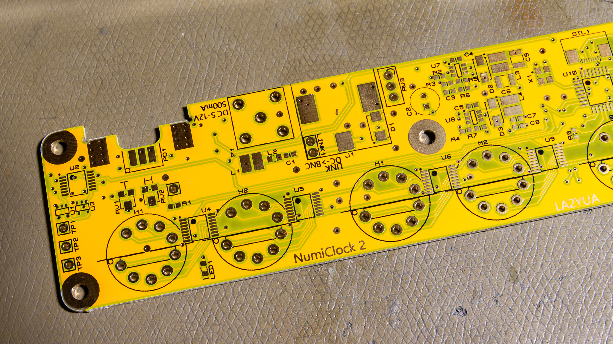
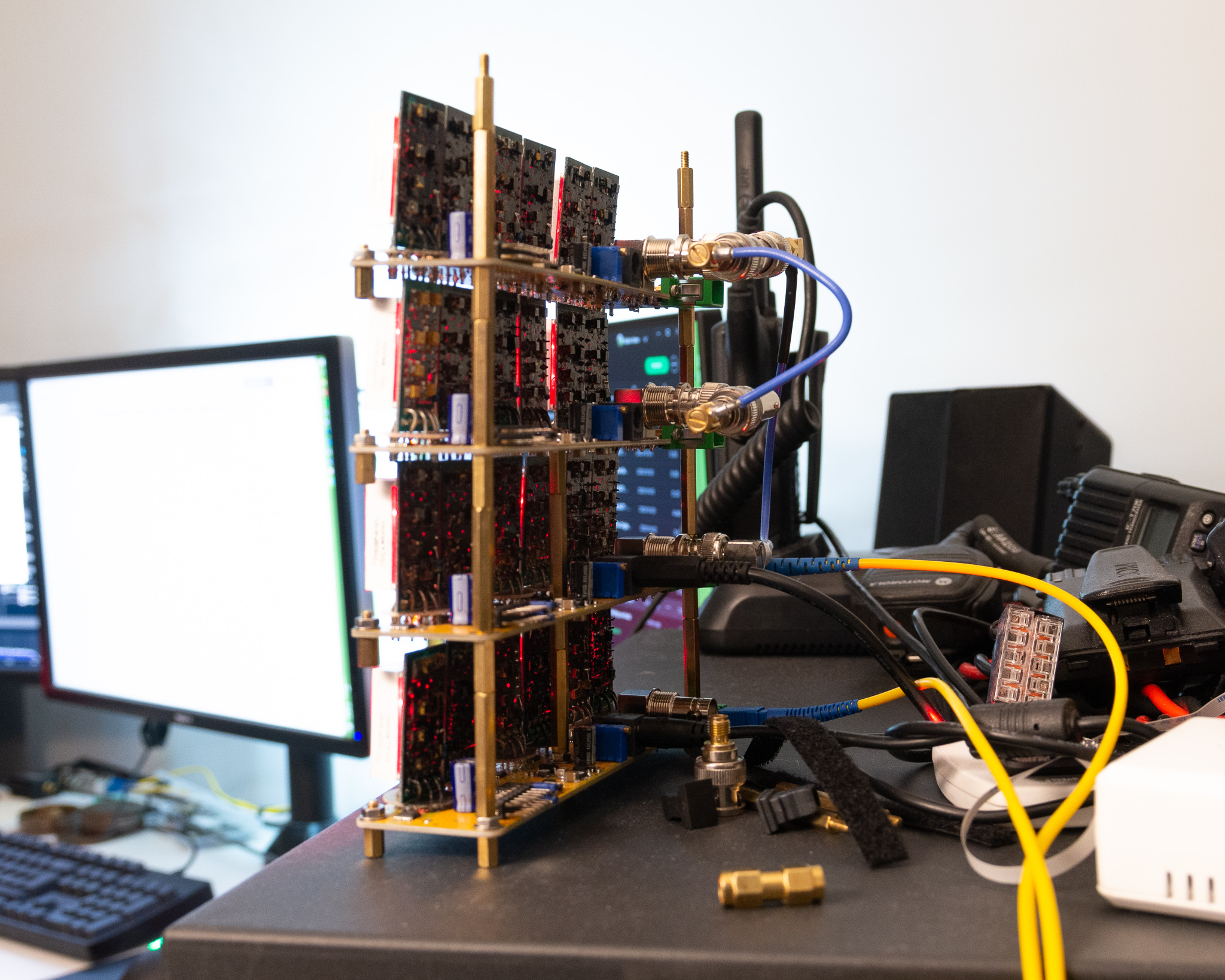
The new clocks are largely the same size and shape as the old ones, but they are slightly shorter due to better design and using smaller packaged devices. The PCB outline is 160⨉40 mm. Hardware cost excluding parts I had for free was around $30 per board.
The PCB is a 4 layer standard stackup from Elecrow (with ENIG). Note that the yellow silk screen is fairly orange and not very thick so areas without copper fill look a sickly green instead - I don't mind the red/yellow colour scheme but it's not for everyone.
Quality was perfectly fine - no issues except they use a low resolution silk screen which is kind of cheap looking.
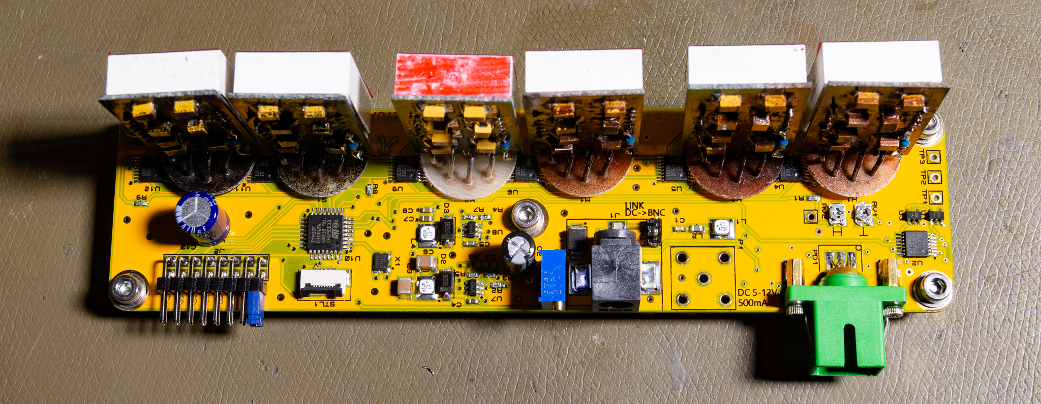
The clock has the same old 7-segment modules, a DC power jack, a BNC I/O port (not fitted in the pictured unit due to some supplier issues), a set of jumpers, and a fiber optic PIN detector removed from a FTTH passive RFoF receiver.
The new clocks use switch mode power supplies for improved efficiency compared to the old design, and the power input has improved protection against reverse and over voltage, as well as fusing.
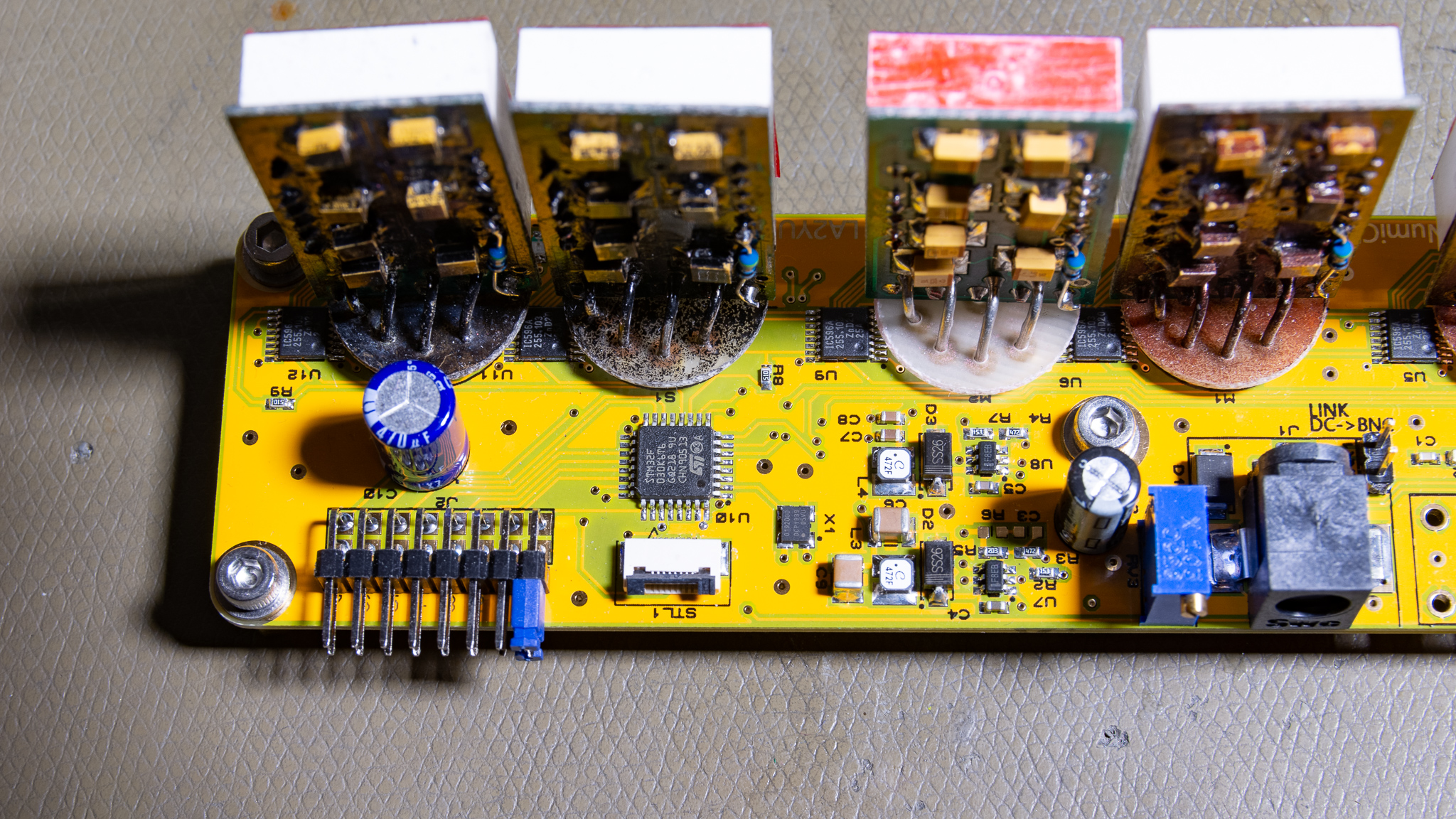
The main processor is a STM32F030K6 in LQFP-32. This MCU is a very capable 48 MHz Cortex M0 processor with an adequate amount of RAM and ROM, the ROM size is somewhat limiting for some applications but it's fine here.
The processor is the only smart device on the board, and runs the entire show. It's programmed using standard C with the STM32Cube HAL. A 19.2 MHz MEMS oscillator is used to provide a reasonably accurate clock for the UART, and to be able to generate a suitable frequency for the FSK detector.
Power
The power supply input is nominally 5-12 V, below around 6-7 V peak brightness is not available due to the dropout voltage of the regulator and series diodes. Above 15 V a TVS + Polyswitch fuse protects the device against overload. This range is very convenient since they can be powered off USB when that's available, and a 9-12 V power supply can be used elsewhere.
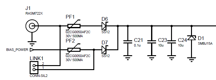
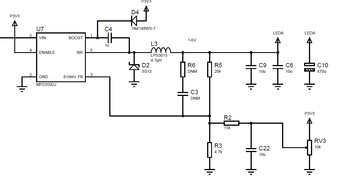
The board has a 3.3 V rail for the MCU and all digital electronics, and a manually adjustable power supply for the LED anodes. This can be adjusted from 2 to 7 V to allow for a wide range of brightnesses (though the brightness matching is poor at low brightness). I used MP2359 1 MHz non-synchronous buck converters for both supplies, these are great little 1 A supplies for the 5-18 V range.
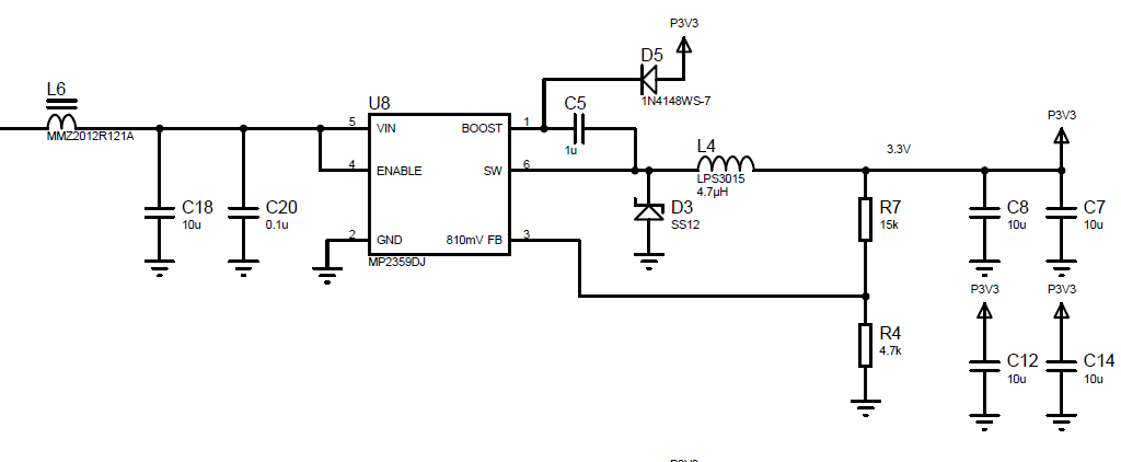
Worth noting: the boost capacitor is nominally 100 nF, I always use a 1 µF or larger boost cap + a backfeed diode with this chip when operating at 5 V input. Otherwise it may lock up during startup and give an unregulated low voltage out.
Display Drivers
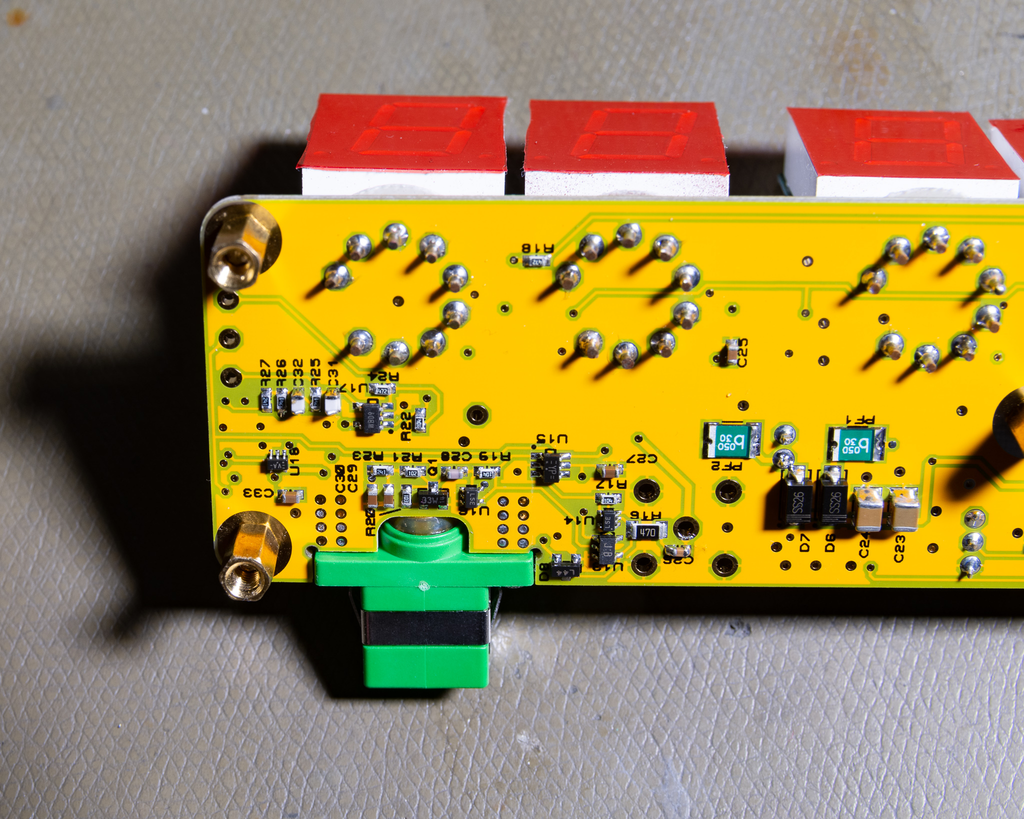
The display drivers used to be 74HC595s in series + driver transistors (the LEDs may float above 5 V, and pull up to 20 mA per segment which would overload an HC output driver). To save space (a lot of expensive board area) I switched to Nexperia NPIC6C596, these are basically 74HC595s with a 30 V/200 mA open drain output transistor. I also switched to a TSSOP package to save space here. The cost is also very low when you're buying 100 of them.
The drivers have 8 outputs, and these are 7 segment displays with a decimal point so that's perfect. As can be seen above the modules actually overlap the driver somewhat but this is fine. The routing is based on what's most efficient (no vias etc.), so the MCU has to shuffle some bits around when generating the display data.
The modules originally came in decimal point or no decimal point versions, I modified all my modules with an extra resistor allowing direct control of the decimal point. This can be seen in some of the pictures.
Optical System and FSK
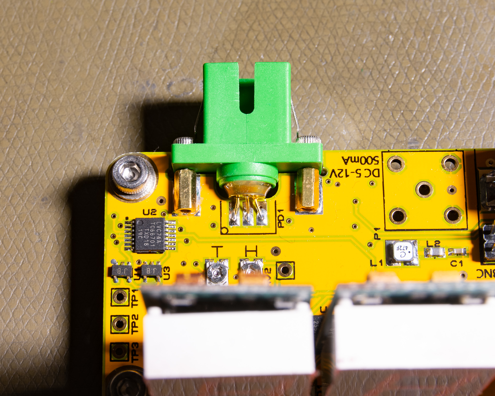
The optical input is just a PIN diode glued in to an SC housing, this is salvaged from a passive FTTH receiver. I used M2 brass spaces soldered to the board, screwed in the module, and bent the leads down. This assembly method was fairly quick and easy, and very cheap.
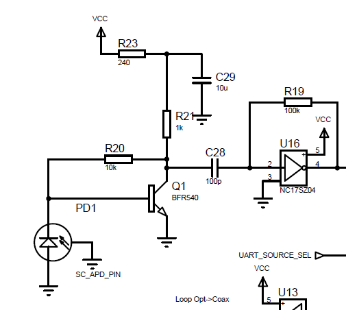
The amplifier for this diode is extremely simple, the diode is operated in photovoltaic mode, and a single RF transistor with DC feedback gives around 10 kΩ gain with a bandwidth of around 30-40 MHz. Typical signal strength is around 200 mVp-p after this. The signal is AC coupled to a standard LVC type 7404 inverter gate with a resistor feedback (self oscillating). This will amplify the signal into a fairly perfect square wave suitable for detection.
Some basic tests indicate that the minimum optical power at 1310 nm is around –20 dBm, and the current system with a 1:8 splitter results in around –15 dBm to the clocks (~–5 dBm source power), which is an acceptable link margin for an optical system. The amplifier is sensitive to overload, so more than approximately –10 dBm can cause issues.
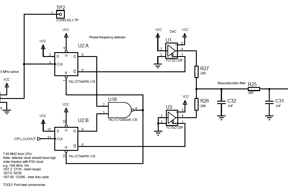
The phase frequency detector is built using the classic double D-latch + NAND gate reset feedback topology, using 74LVC74 and 74LVC1G00 (single element NAND) ICs. The up/down outputs are fed to 74HC125 type (single gate) tri-state buffers, one connected to high, another to low. There's series resistors from each output going into the reconstruction filter.
I suspect 10 MHz is a bit too fast for this detector to work well at, since the output level when idle is somewhat lower than the ~3V it should be, but it gives a good stable SNR.
Since the local oscillator from the MCU is not precise, the choice of frequency matters. If a synchronized clock were used a 5 MHz reference frequency would work fine for the 10/1 MHz FSK. However, there are some beat frequency issues at the output when operating unlocked in this mode.
I did some experimentation and found that using something with a high order fractional ratio worked better. In this case I chose to use 5.2 MHz instead of 5, this decision is the reason I used a 19.2 MHz oscillator for the system. The internal 8 MHz oscillator in the MCU can't be used to generate 5.2 MHz with the master clock output.
The internal oscillator is also very imprecise compared to the MEMS oscillator I chose, but this issue could have been resolved by auto-trimming the oscillator based off the time code.
Digitization
The reconstruction filter is a 2-pole RC filter with a cutoff suitable for the UART baud rate. After the filter, a MCP6561 high speed (sort of) CMOS output comparator is used to slice the signal into a square wave for the MCU.
This comparator is set up with an adjustable threshold and hysteresis level, this was done to ensure that I wouldn't spend days swapping resistors to get those right. Two trimmers are used to implement this function.
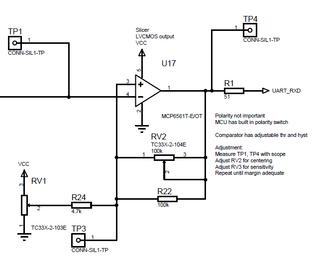
There are 4 test points available here to allow easy trimming. These are: FSK signal (square wave), the PFD output after filtering, the comparator reference input, and the comparator output.
The primary adjustment is done by using an oscilloscope to look at the PFD output and the comparator reference input. This shows the signal and the thresholds (with the hysteresis). By overlaying these signals, the adjustment is very easy to perform.
The BNC Plug
I haven't really mentioned the BNC port, this is a fairly obvious extension to the basic fiber optic system.
I only had 6 BNC plugs, so at the time of writing I'm waiting for a shipment of some more plugs for properly finish off all the clocks. Turns out I had more fiber coupled PIN diode assemblies than BNC connectors laying around.
The BNC plug can be used as a power source (via a on-board bias-tee), it's ORed with the normal power input.
There is a jumper on the board which connects the DC input to the BNC power without any of the series diodes. The fuse is not bypassed for safety reasons. With a 12 V power input driving 4 other clocks is not an issue with typical brightness levels.
Further, there are digital switches which allow selection of either the optical signal or the BNC as the signal source. By default a clock using optical input will also drive the BNC as an output.
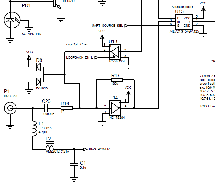
This means that one clock with power + optical input can drive several other clocks over a standard 50 Ω cable with signal and power. In principle the power and data can also come from different sources.
This system is intended to provide some additional flexibility, e.g. multiple clocks can be co-located without separate power and fiber optic links. It can also be useful in future cases where e.g. a clock + a frequency standard receiver may be co-located. The frequency standard may be powered directly and have an optical input, while the clock can be connected to the BNC.
Since there's no slew-rate limiting on the BNC output it's not a great system to use over long distances due to EMI and waveform distortion where multiple drops are used. It's mostly intended for very short runs e.g. within a single rack (where common mode issues aren't huge).
The Transmitter
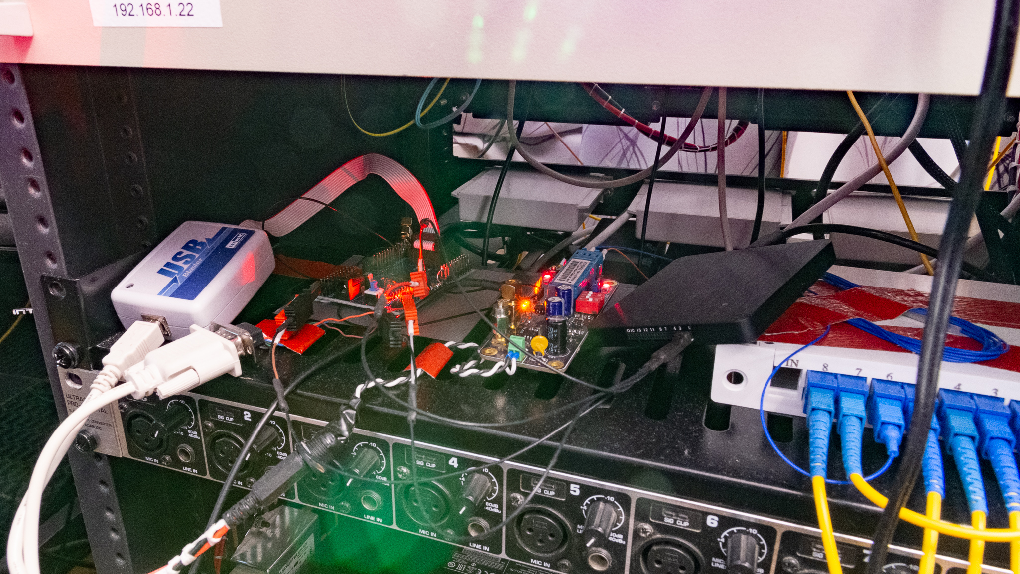
The transmitter for the system is currently a prototype, it's based off a MAX II CPLD evaluation board, the existing 10 MHz and GPS clock system with some software fixes, and some previously built SFF module breakout boards.
The intention is to make a much more sophisticated distribution source, including redundant source types (e.g. multiple GNSS systems, radio clocks, and internal holdover with battery backup). This is a fairly significant project, so it's not the highest priority right now.
The MAX II CPLD is fed with an external 10 MHz clock, a UART timecode signal, and a 1PPS signal.
The UART signal is set to 100k-8O2, this was chosen to have an integer ratio with the mark/space frequencies. The relatively high frequency also ensures that the timecode transmission time is short, reducing the time the FSK signal is not 10 MHz to below 10 ms per second.
The use of Odd parity was inherited from the old Lucent system, and 2 stops bits is used to give some extra margin against sampling-jitter since the UART transmitter uses DMA with minimal word spacing.
The CPLD resamples the UART data at 1 MHz, and uses a basic mux to select between 10 and 1 MHz for the output.
The 1PPS UART signal is generated by the CPLD to avoid any software induced jitter in the signal timing. The choice of baud rate and parity means that a valid 0x00 byte transfer simply means keeping the line low for 9 bit periods (and guaranteeing it remains high some time before and after to give valid start/stop bits). A 4 bit counter + some latches is all that's needed. The design shown below is not optimized for gate count, but is very understandable and easy to modify.
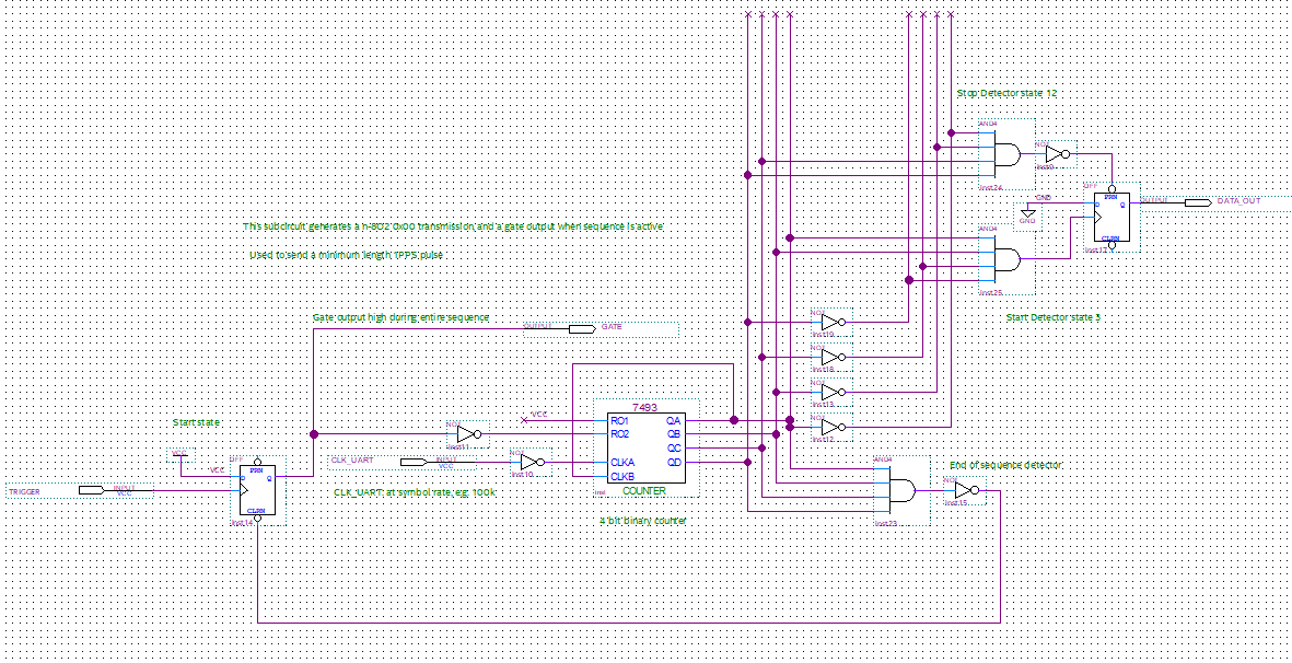
The CPLD also resets all it's internal clocks when the 1PPS pulse is detected, this is done to reduce jitter caused by e.g. the 100 kHz clock generator not being aligned to the 1PPS edge.
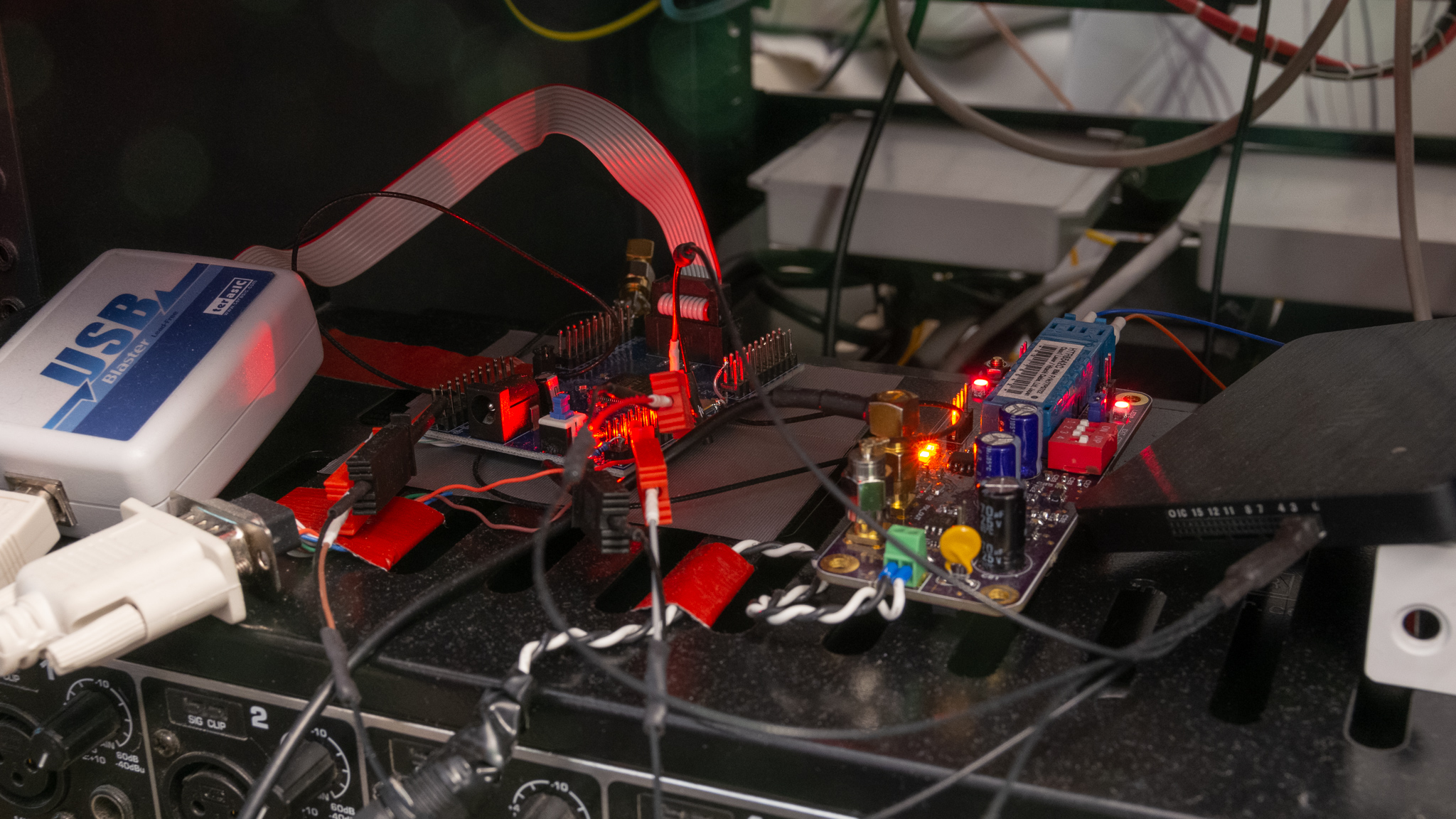
The generated FSK signal is fed to a previously made SFF module driver, which is connected to a passive 1:8 splitter which feeds the clocks.
The final system will likely include at least 4 inputs and outputs (using the same optical system for the time sources is very practical). This will allow up to 32 clocks to be driven directly from the source with passive splitters. I might also include a high power output capable of driving two 1:8 splitters in series (up to 64 clocks driven from a single output).
Future Work
I plan to make several improvements to the system, though the clocks are "done" for now except software updates.
As outlined above a suitable distribution system with redundant inputs and holdover is definitely planned.
A compact source using a basic GNSS receiver is something I might make e.g. for use in the office. I might even include a 10 MHz disciplined oscillator just for fun but primarily this would be to drive the clocks.
A basic 10 MHz distribution amplifier as outlined above is planned, this will be used to feed some radio receivers and measurement instruments. It should be fairly simple project (VCTCXO + CPLD + MCU), as I have built similar devices before.
An expansion board for my Meinberg DCF77 PCIe receiver card something I would like to build, this would take the frequency reference + timecode + 1PPS from the Meinberg card and generate the FSK signal the clocks use over fiber. This output could be routed directly to the clocks if required, but would primarily feed the distribution system as a redundant source.