The 3021N Synthesizer (Part 6)
The 3021N Synthesizer is a very complex part of the original radio. It's almost sad to replace it, but I needed the room to fit new power supplies. The synth was designed in the fall of 2020.
Table of Contents
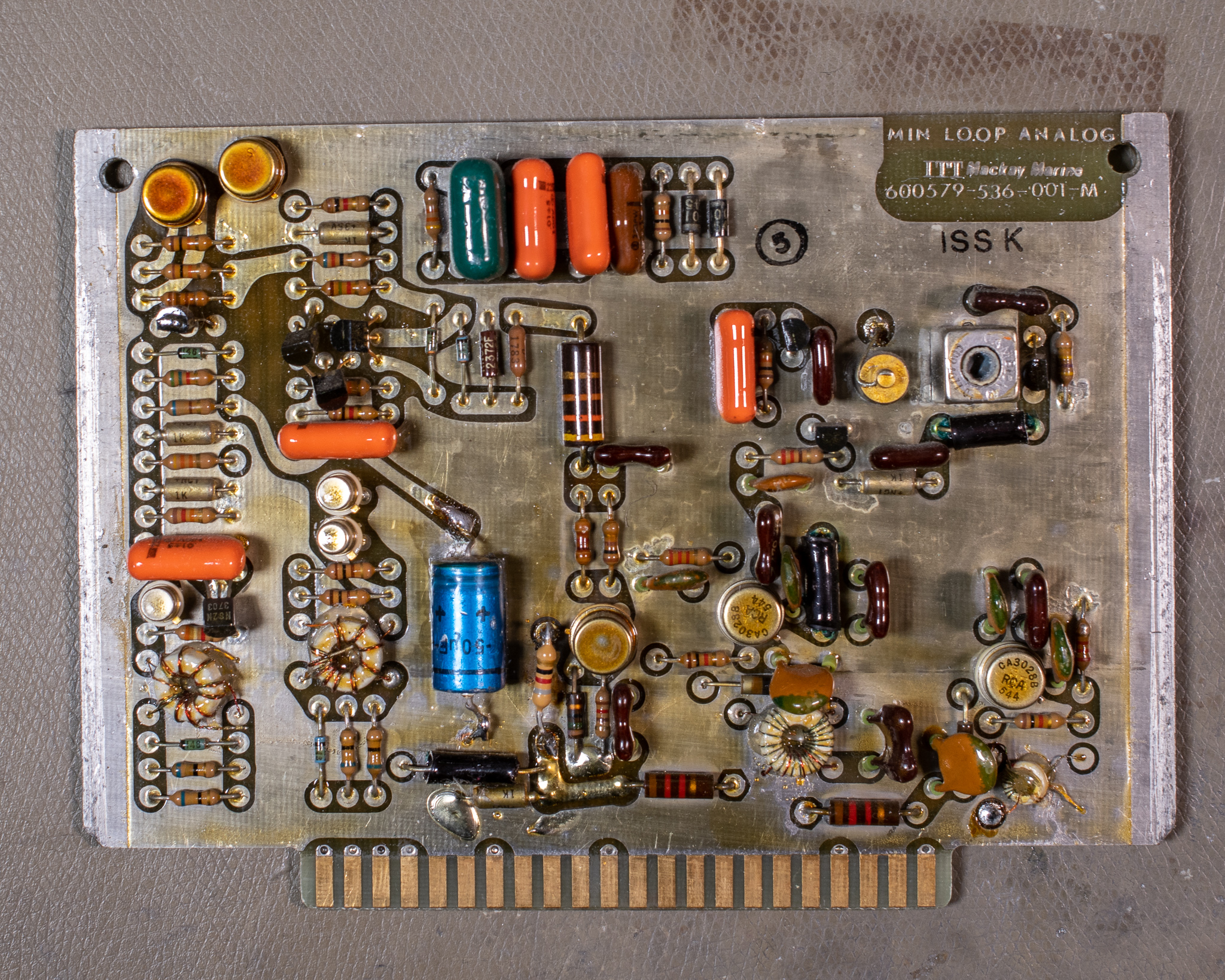
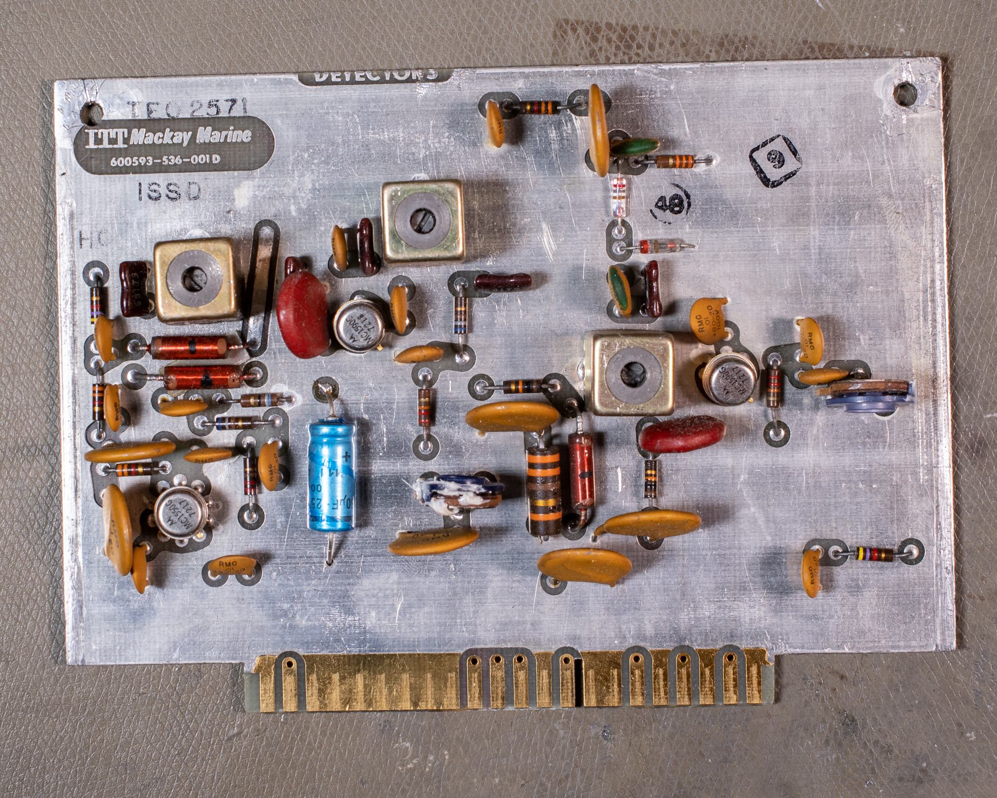
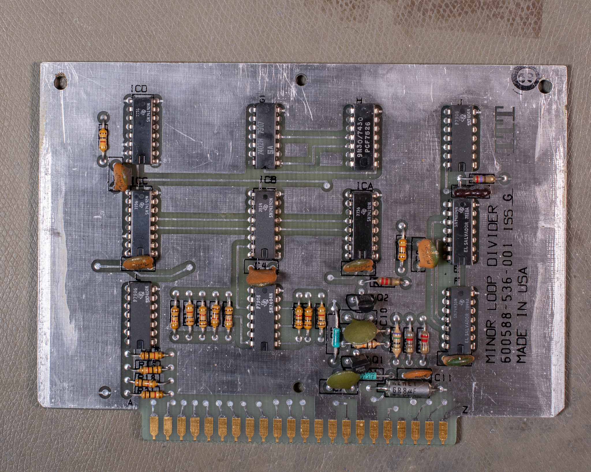
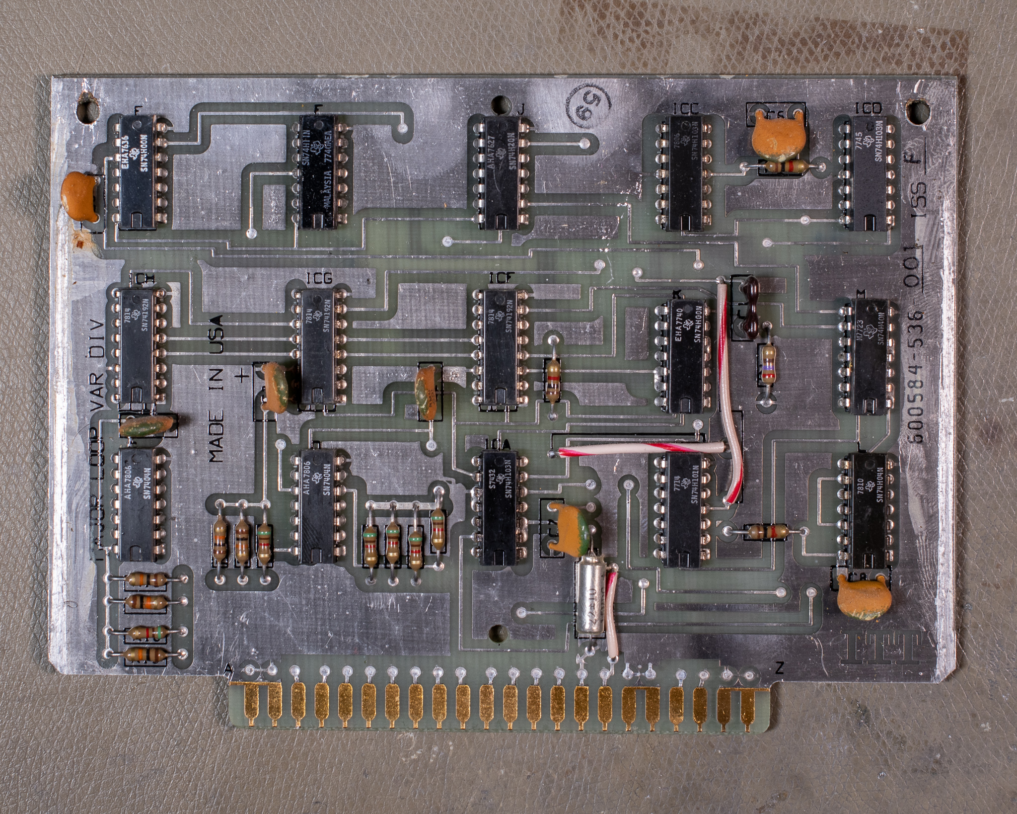
The Original Synthesizer
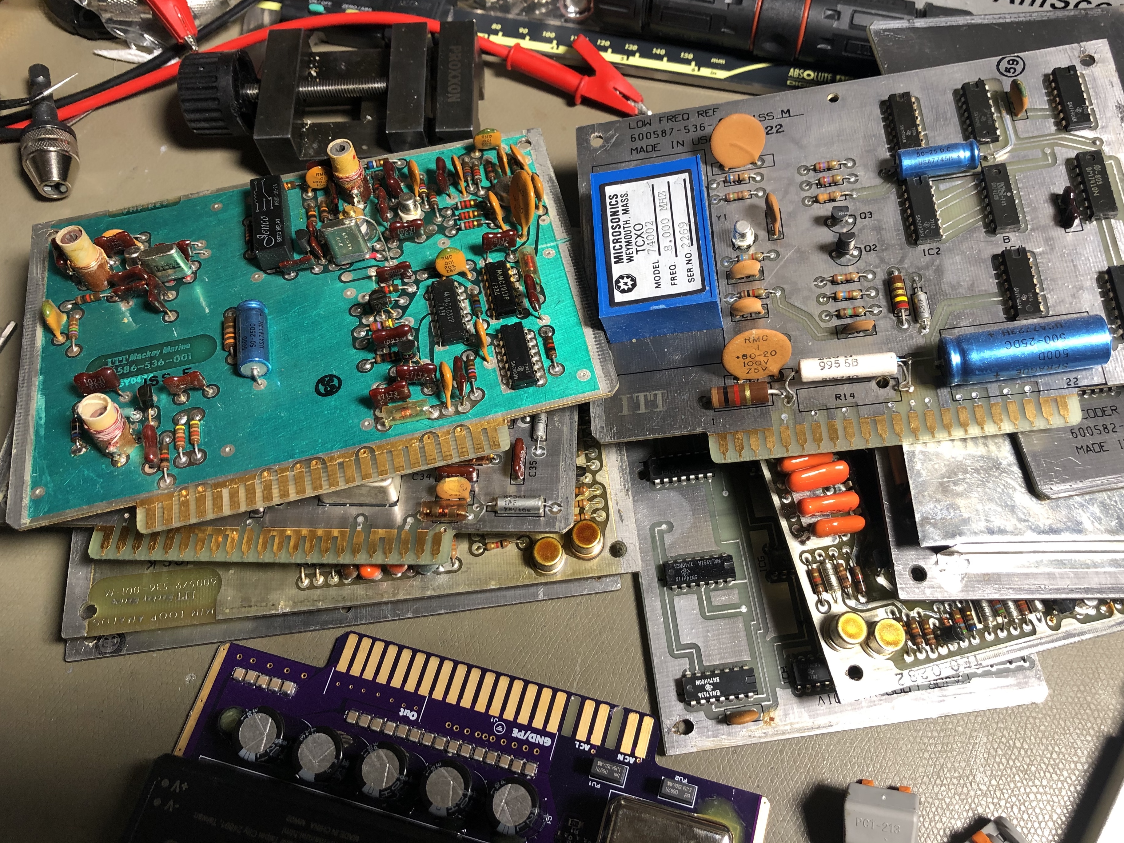
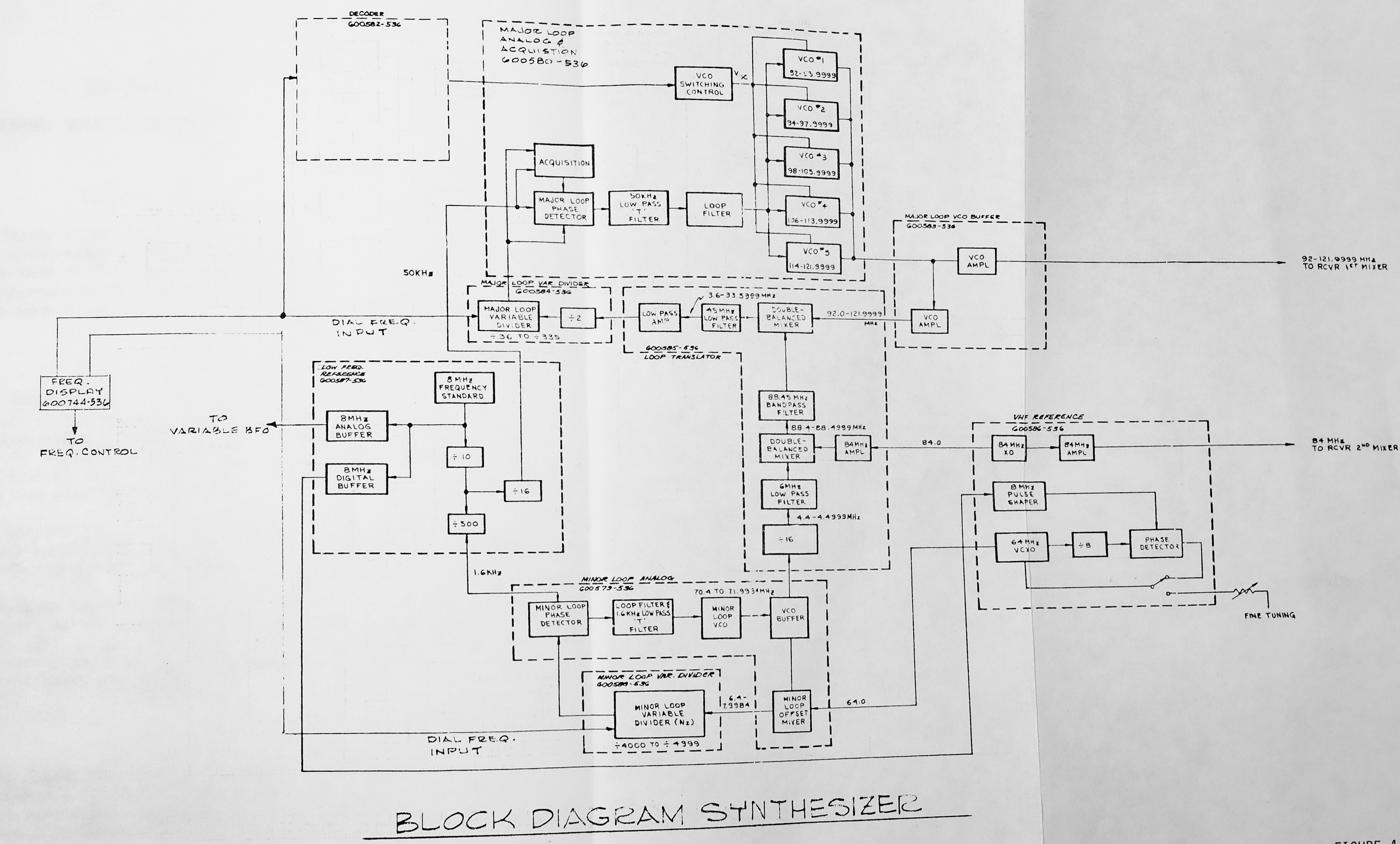
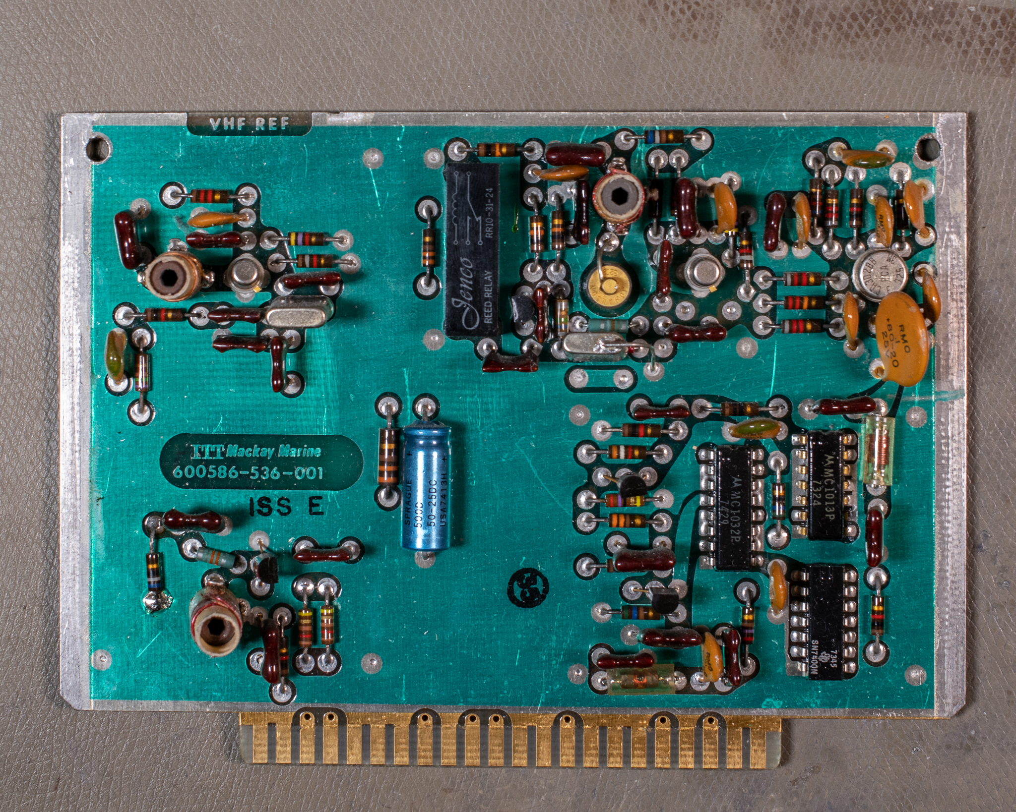
The original synth was a masterpiece of design, it's a 100 Hz step synth covering approximately 92.015 to 122 MHz for the LO1 and a fixed 84 MHz LO2 output. The synth uses several VCOs and VCXOs to perform various translation steps, but in the end the entire synth is in fact controlled by a single 8 MHz TCXO.
In my experience the original TCXO was quite good, considering the age and type. The synth is controlled by a set of BCD digits generated in the STL card.
The 8 MHz output was used for the fixed beat frequency oscillator, and when originally installed the new demodulator card used this as the clock reference for the digital circuitry.


Specs & Design Rationale
I realized at some point that if I could remove the old synth, I would have nearly infinite room for whatever else I wanted to add. The main thing I wanted to add was new power supplies, as the old supply took up most of the rear panel of the radio.
The basic specs of the old synth was:
- 92.004-122.004 MHz, 100 Hz step LO1, around 0 dBm
- 84.004 MHz fixed LO2, around 0 dBm
- 8 MHz reference clock

The synth was designed to meet this spec (except 20 MHz replaced the 8 MHz), with the introduction of the new 1st Converter (future work) the frequencies will be revised:
- 100.215-160.2 MHz, 100 Hz step LO1, more than -10 dBm
- 100.176 or 100.224 MHz fixed LO2, more than -10 dBm
- 20 MHz reference clock
- External 10 MHz disciplining with automatic adjustment
The old synth used a VCTCXO of fairly good quality, made by Microsonics. I decided to add an additional requirement for a 10 MHz input and automatic VCTCXO holdover trimming.
The solution uses a MC145170-2 PLL IC, whose phase-frequency detector (PFD) output is digitised by a STM32F030 MCU, a digital loop filter then controls a PWM-DAC which sets the VCTCXO frequency. An F-RAM IC is updated with the last stable DAC code, and if the external 10 MHz is removed, the DAC will use this setting. A potentiometer can be jumpered in to offset this value, allowing for manual trimming as well.
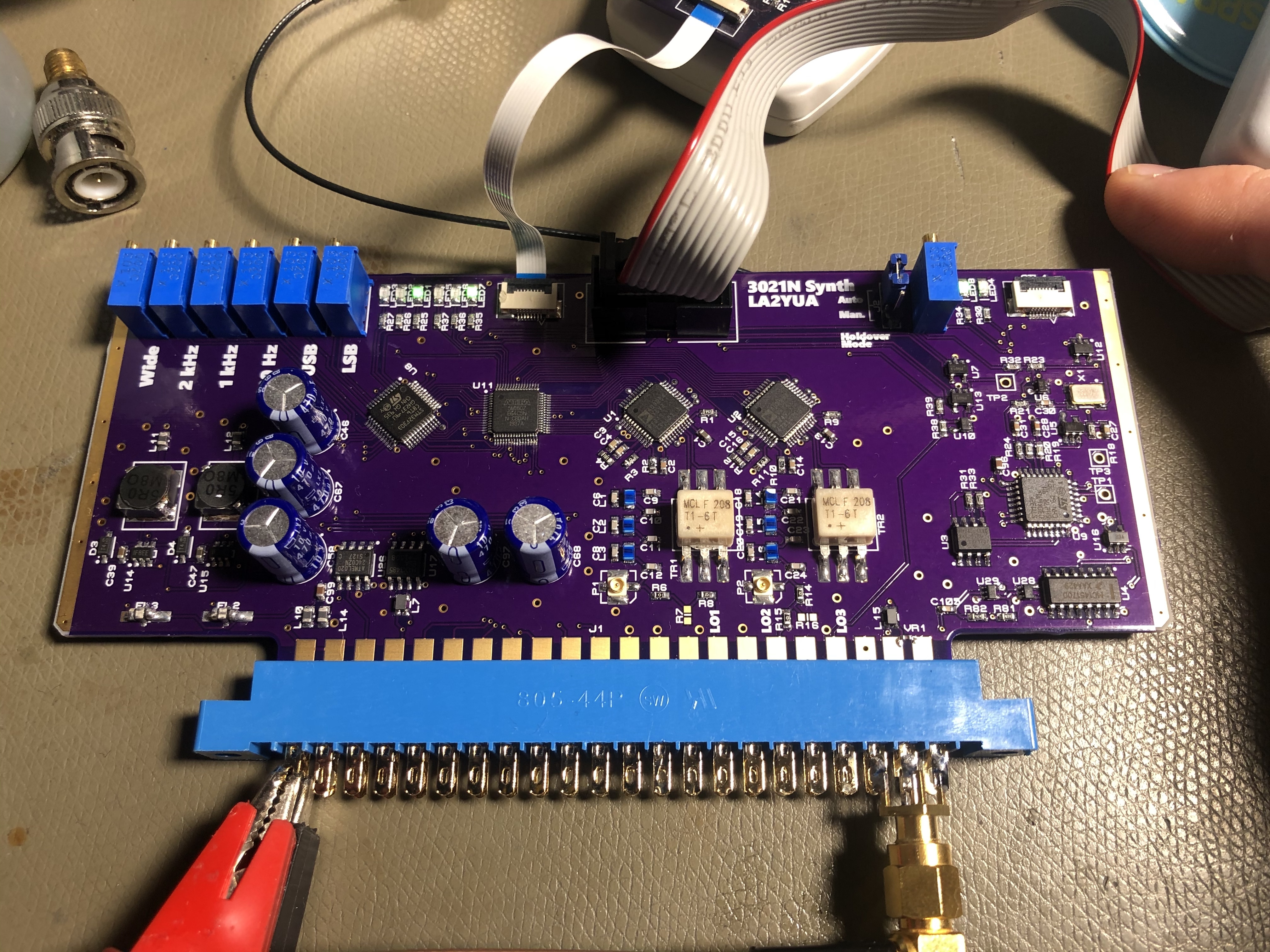
I found that some AD9954's were available, and two of these are used to make the two LO's. These are 400 MSPs DDS sine wave generators, with 32 bit tuning words they can make any frequency from 0 to 200 MHz with around 50 mHz resolution. These DDSes are controlled via SPI, and fed with a 20 MHz VCTCXO that makes up the main radio time base. Internal multipliers make an internal DDS clock at up to 20⨉ multiplication.
The CPLD also acts as a receiving shift register, receiving data from the STL card over SPI as a 24 bit tuning word. This signal is received periodically, and whenever the STL changes the commanded frequency. The CPLD receives the transfer and generates an interrupt to the MCU, which then reads the tuning word and commands the DDS to achieve the given frequency.
The whole thing is optimised for speed, in order to ensure that the actual receiver frequency of the radio always matches the display without delay, and that individual frequencies aren't missed when quickly scanning. This may seem silly, but it's definitely worth the effort and basically required for a good user experience.
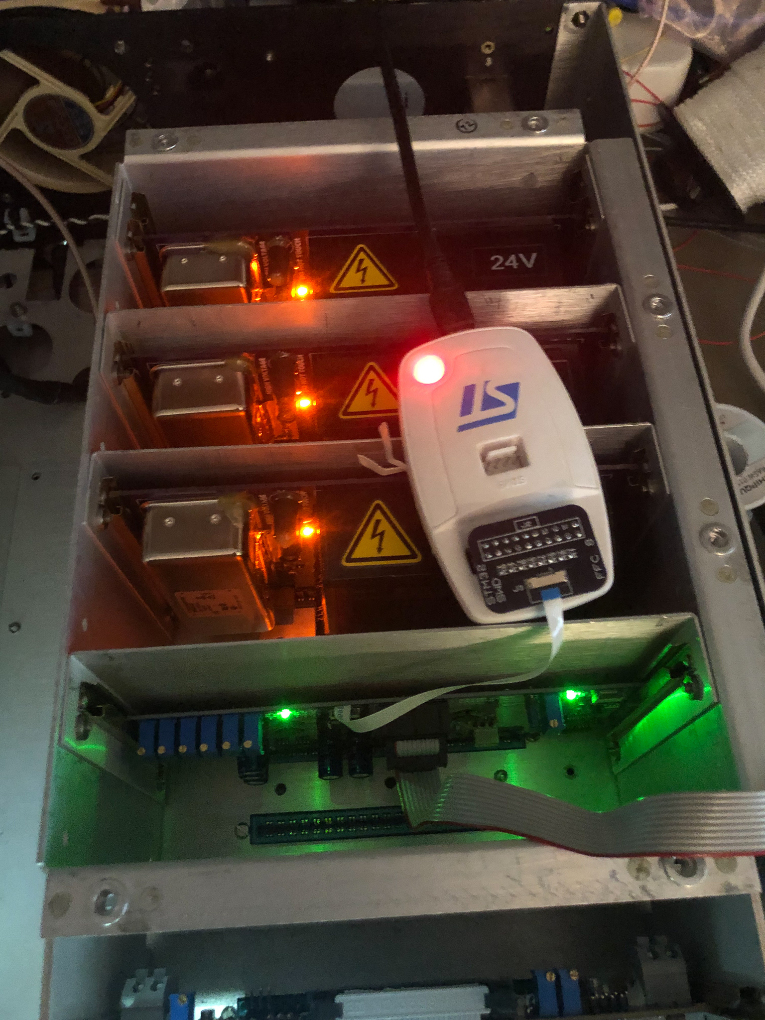
Seen above is the Synth card along with the new power supply system, but before OCXO installation and RF section replacement. Green LED's were used for some reason (instead of the superior orange LED), one of the LED's toggles state every time a frequency update is received, making for a cool light show.
I use an 8 pin 0.5 mm FFC cable for SWD debug of STM32s, it's a very cheap and convenient connector.
DDS Spurs
An issue with the DDS generators is that they tend to produce spurious frequencies given by the interaction between harmonics and subharmonics of the output and reference clock. In order to ensure that these spurious frequencies stay as far away from the actual tuned frequency, the reference clock to the DDS is altered depending on what frequency range is commanded. This unfortunately takes around 1 ms to do, but this only happens every 4 MHz or so, and 1 MHz of hysteresis is used.
A redesign would likely re-evaluate the choice of reference frequency and DDS chip to make this even better. Alternately, a filter-bank could be added. As long as spurious frequencies stay sufficiently far away they are unlikely to cause issues, and the pre-selector can be used to attenuate any that do cause issues.
LO2 Offset
The synthesizer includes a set of potentiometers which were intended to support filter-specific LO2 tuning, to basically offset the IF2 frequency to match the actual crystal filter response.
This idea was dormant for a long time, but upon actually testing and measuring the crystal filter performance it was found that IF shifting would not yield a sufficient improvement to justify the effort.
The plan was to use a dormant RS-485 link between the Synth and Demod cards to inform the synth of the filter in use, and to inform the demod card of what frequency offset should be applied when detecting IF2.
The result of this test was that a design effort was started to replace the entire RF section of the receiver with a new design which had precision filters. This is the subject of future articles.