
Wide Band Radio over Fiber System
Radio over Fiber is a well established concept by now, this is a look at a wide band multi-antenna receiver system with radio over fiber distribution.
Table of Contents
Background
See also my first RoF system, the HF over Fiber system.
Radio over Fiber (RoF) has a number of clear benefits, and a multitude of downsides for most users. For some users the benefits outweigh the downsides, and in my case the ease of distribution and sheer fun of building it makes it worthwhile.
To summarize, RoF eliminates RF noise issues in complex systems by virtue of having nearly infinite galvanic isolation. The downside is typically cost, complexity, and linearity. In my experience so far, the linearity issues do not seem to be significant, even for a system of high complexity.

The problem to solve with the system described here is:
- Want to receive multiple frequency bands in the 100-1600 MHz range
- Want to use the optimal antenna for each frequency band and use case
- May want multiple SDR receivers per antenna
- Also want to use an interactive SDR to monitor all frequency bands of interest without antenna switching
Surprisingly, these problems were solved using RoF!
Using coaxial distribution would simplify some aspects of the design, but severely complicate others, especially the need for wide band high port-count RF splitters.
System Overview
The overall goal has been set, the implementation can then be designed. I can then specify some specific antennas/filters I want access to:
- 118-174 MHz VHF air, ham, and LMR
- ~220 MHz (Band III) for DAB (nice to have, not required)
- 400-406 MHz for small satellites and weather balloons
- 420-450 MHz for ham and LMR
- 1090 MHz for ADS-B
- 1200-1300 MHz (23 cm ham)
- 1000-1700 MHz for GNSS bands 1, 2, and 5, geostationary L-band services, Iridium
These signals will be routed to:
- RTL-SDR receivers
- MSI SDRs where relevant
- PlutoSDR/AirSpy R2
- GNSS receivers
I decided to build a primary combiner box which can accept all these inputs, summing them for transmission on a single laser transmitter, and which includes adjustable gain per antenna source. This adjustable gain is critical since the noise levels and LNA gains for various antennas may not be optimal.
Risk Reduction Phase
A major uncertainty was how critical the system would be to the antenna gain, would this system require AGC for all channels? Would I just make a pile of useless expensive circuit boards with or without it?
In order to reduce this risk, a test system was set up using a pile of modules which ran for a few months in the summer of 2021. This system did not use AGC, but no major issues were observed because of this. If a local transmitter were active this would usually saturate the system, but since this only occurs when I'm talking on a radio this is usually fine.
It also showed that some adjustable gain functionality per channel was essential since combining a pile of active antennas with as much as 40 dB difference in gain would result in significant issues.
Another issue identified was that the typical set of antenna→filter→preamplifier is fine for single antenna systems, but the output noise of high gain LNAs is wide band in most cases.
This adds output noise at "all" frequencies, and it became clear that a topology of antenna→filter→preamplifier→filter would be required.
Based on this test run, I was able to go ahead without implementing AGC, and manual gain was selected. An option for adding AGC later was included. The main risk with integrating AGC was the wide bandwidth, making a single solution for the entire frequency range difficult to design.
Implementation
The implementation was informed by previous work including the risk reduction tests.
To prevent issues with wide band amplifier noise, I decided to add one band-pass filter to each antenna input, which roughly limits the port bandwidth. Further I decided to use an output filter per input to the combiner as seen below to band limit the noise further.
Each antenna source is provided with a +5 V bias, and is expected to be pre-filtered and amplified. A target noise figure of the antenna inputs to the combiner was set to around 4 dB, and the antenna preamps must provide at least 10 dB gain to be optimal.

Based on the above considerations I arrived at the above configuration, consisting of 8⨉ antenna inputs, which is input to 4⨉ combiner/amplifier (and gain control) units. These units then feed a 4-port combiner, the output of which is amplified and applied to a high power DFB laser.
These components will be looked at more closely below, with the exception of the antenna/preamps, which is considered to be fairly standard and outside the scope of this system. Most users already have equivalent preamp/filter functionality already, and while some custom design was done there it is not ground-breaking. Some details are available near the end of this article.
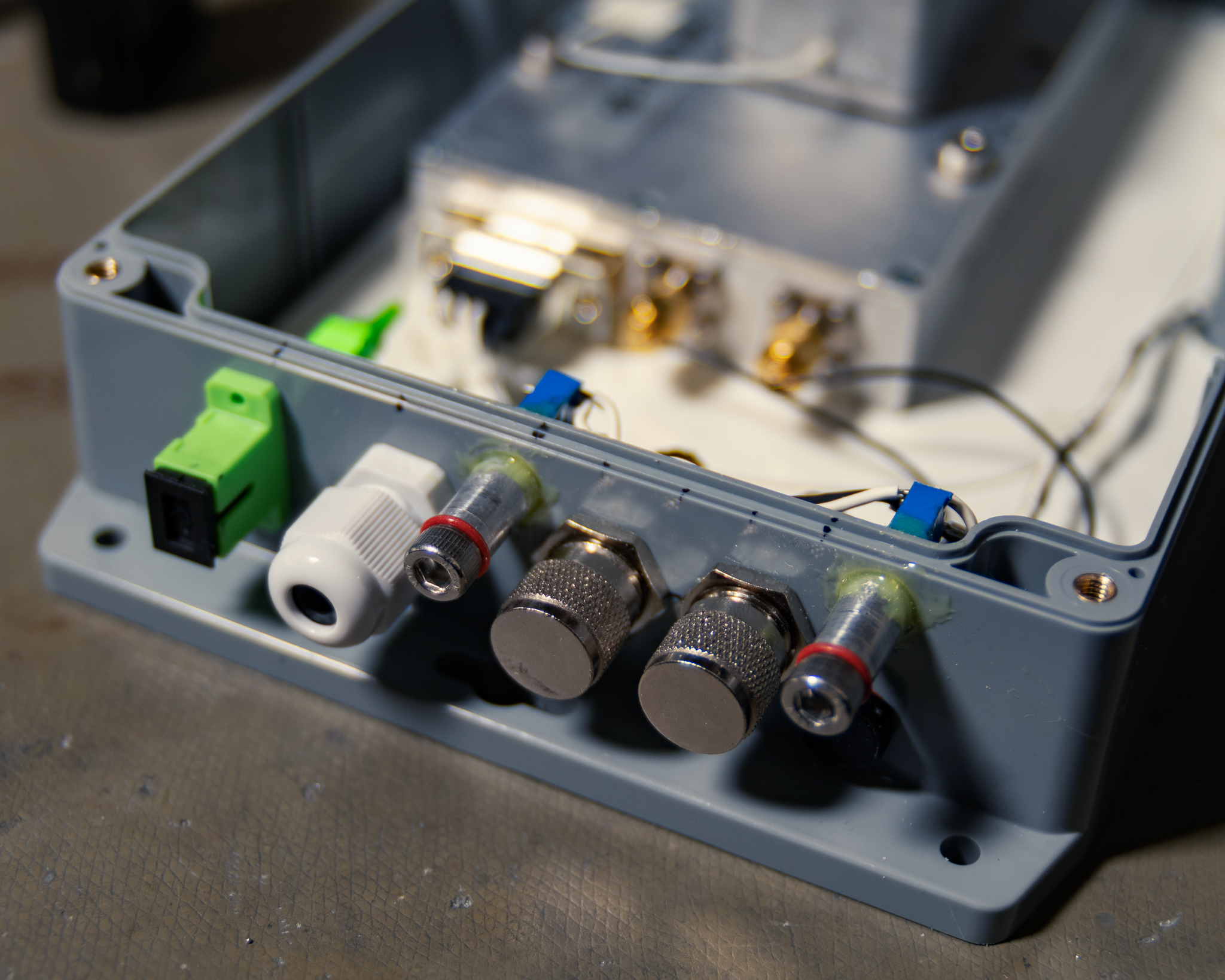
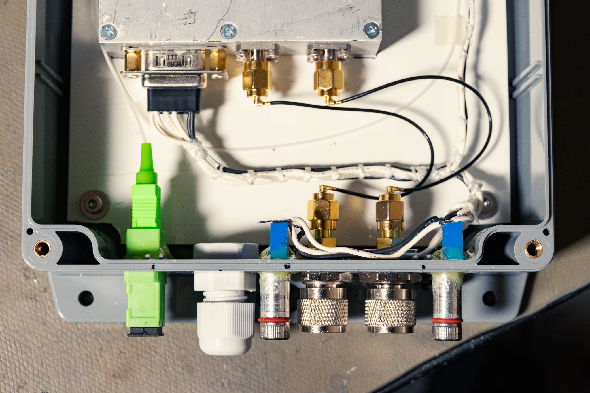
The physical implementation was done using an unshielded plastic enclosure made by Bud. Since the outer enclosure is unshielded we obviously need shielded enclosures for all the subassemblies to prevent massive interference from 4/5G signals.
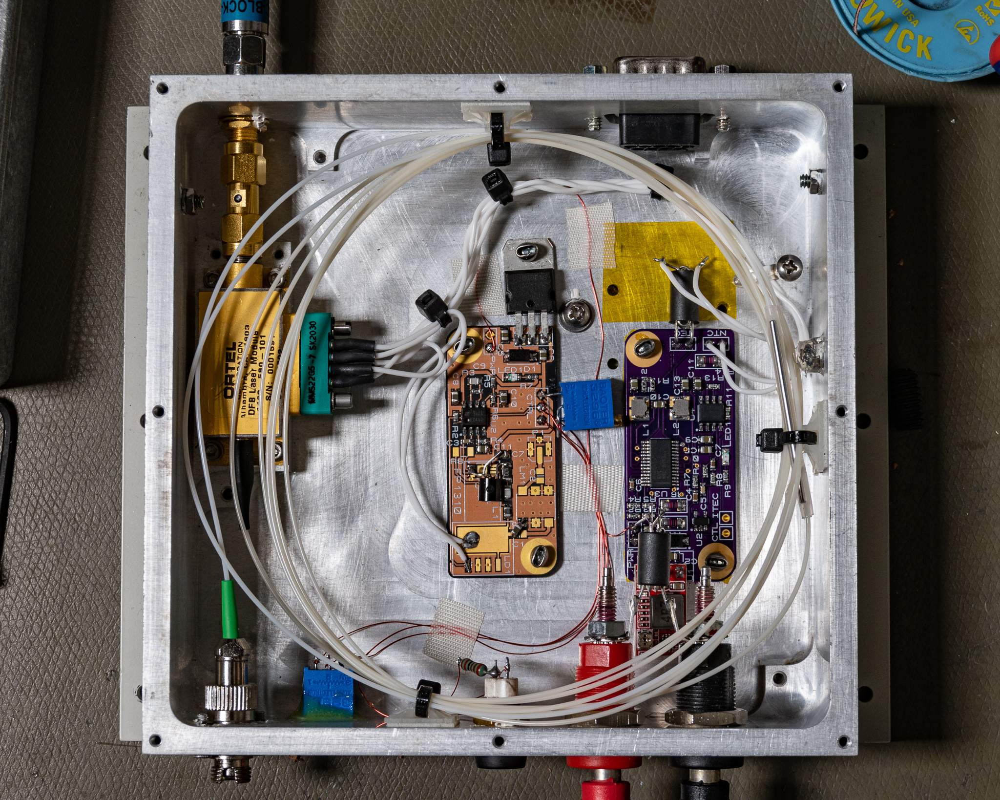
Above is a picture of the assembly, showing from top left: Laser Preamp, Laser Module, stack of 4 combiner/amplifiers, and the 4-port combiner. To the bottom left is the power inlet and distribution.
The gain control panel is installed on top of the combiner/amplifier stack. It is simply an aluminium plate with 8⨉20-turn potentiometers glued in, this generates the control voltage for the attenuator control for each channel. This was later replaced with a DAC board.
Power System & I/O
The system originally operated on +14 V, and required around 2 A continuously, mainly to supply the RF amplifiers in the combiner/amplifier boxes.
Power is supplied using shielded twisted pair (audio microphone cable; positive/return + shield, shield and return connected at the source).
Later an isolated DC/DC module was added which output 15 V, this changed the input spec to 10-32 V/~20-30 W fully balanced. The actual DC/DC module is packaged in a (trash picked) shielded die cast enclosure with feed-through capacitors for power I/O, as well as internal common mode chokes and Y-capacitors on both inputs and outputs. The primary purpose of this addition was switch the power source to a 24 V output where more power was available.
The power input was also connectorized with this upgrade, replacing the M16 cable gland shown in a previous picture with a 3-pin "SP-13" plastic connector.
To keep down on the mess when this is left outside I use M16 cable glands to feed the coaxes through instead of having external connectors. This also saves a bit of money.
The fiber connection is an SC APC at the time of writing, as shown above.
A vent gland is also installed to equalise internal/external pressure while blocking ingress of water.
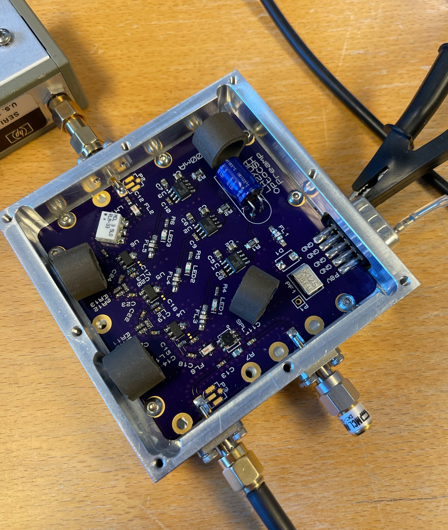
Combiner/Amplifier
The combiner amplifier is a key part of the system, it implements the summation of two antenna signals, with provided 5 V bias to the antenna preamplifier, with adjustable gain per channel.
Another key aspect is the output filtering, which is critical to avoid interference between the different frequency bands.

Seem above is the block diagram, showing two antenna inputs, each provided with a bias-tee to power the antenna preamp. Each combiner amplifier has an input filter suitable for the frequency range in question, limiting any wide band noise picked up from the coax, or generated by the antenna preamp.
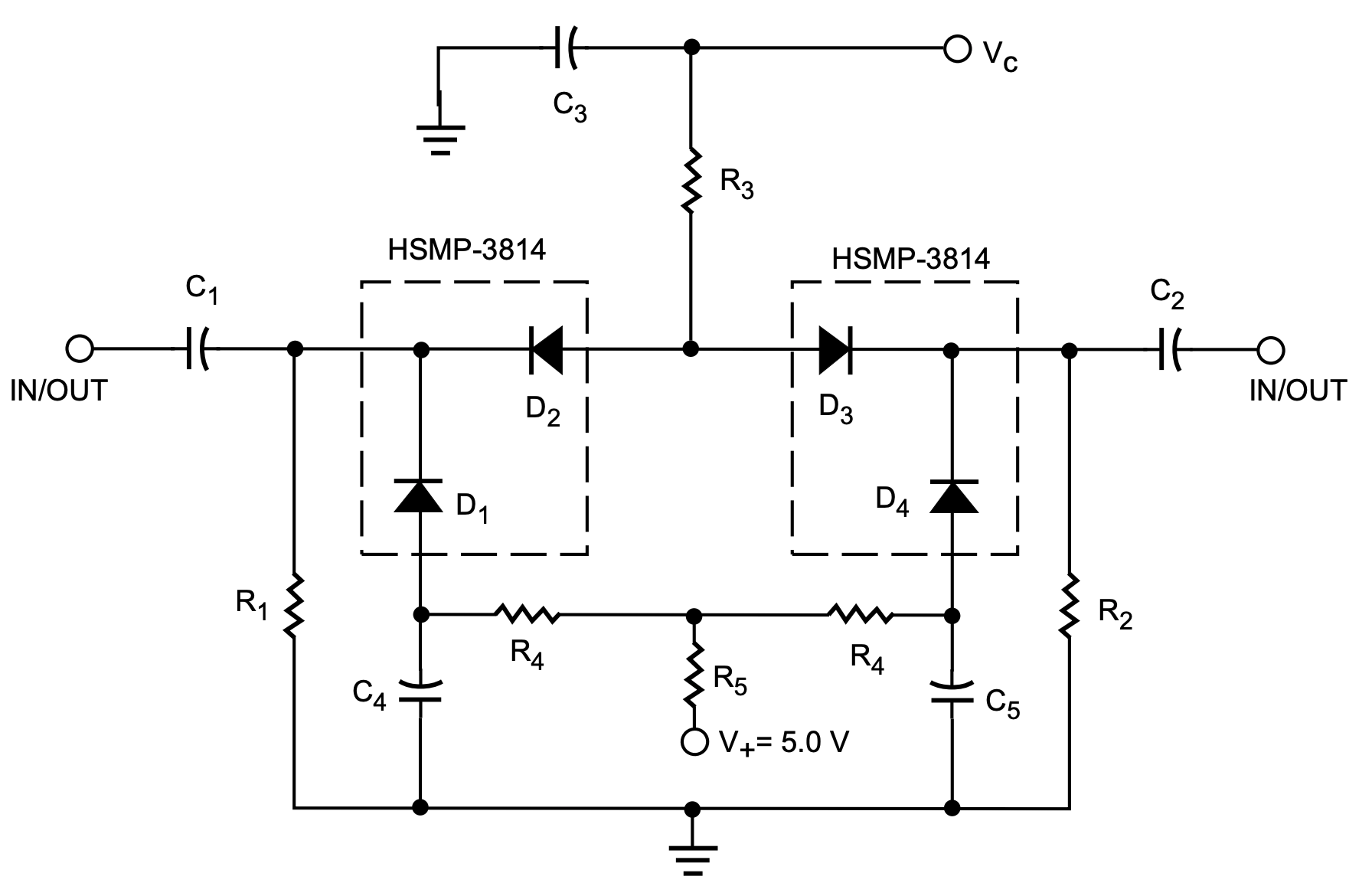
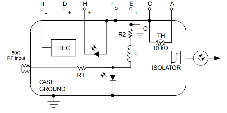
A PIN diode attenuator per channel is controlled using two external control signals, and the signals are combined after attenuation. The design selected is the "4 Diode π Attenuator" as described in HP Application note 1048, the core schematic of which is shown below.
Following the attenuators, the signals are combined using a TCP-2-33W+ "top hat®" power combiner, which adds around 4 dB insertion loss to each signal.
From the input we then have around 3 dB filter losses, and the attenuator likely adds 3-6 dB of losses in the highest gain setting. With the combiner dropping 4 dB, the +18 dB gain of the first stage amplifier is basically spent, so an additional +18 dB amplifier is used after the combiner.
The output is then sent through a band pass filter of the same type as on the inputs. Where two filter types are used, this is the union of the two frequency ranges on the inputs.
The selected enclosure is a reused component from a GSM-R base station, which I had a sufficient quantity of available. This enclosure is machined aluminium, with an included filtered D-Sub connector (only 5 pins available), and 3 SMA connectors.
The same PCB is used for all frequency ranges, only the filters change. If you look closely you can see that there are two filter footprints with jumper resistors to select which is in use. I also added some marker fields to write down which filter is installed, since the LTCC filters aren't marked for frequency.
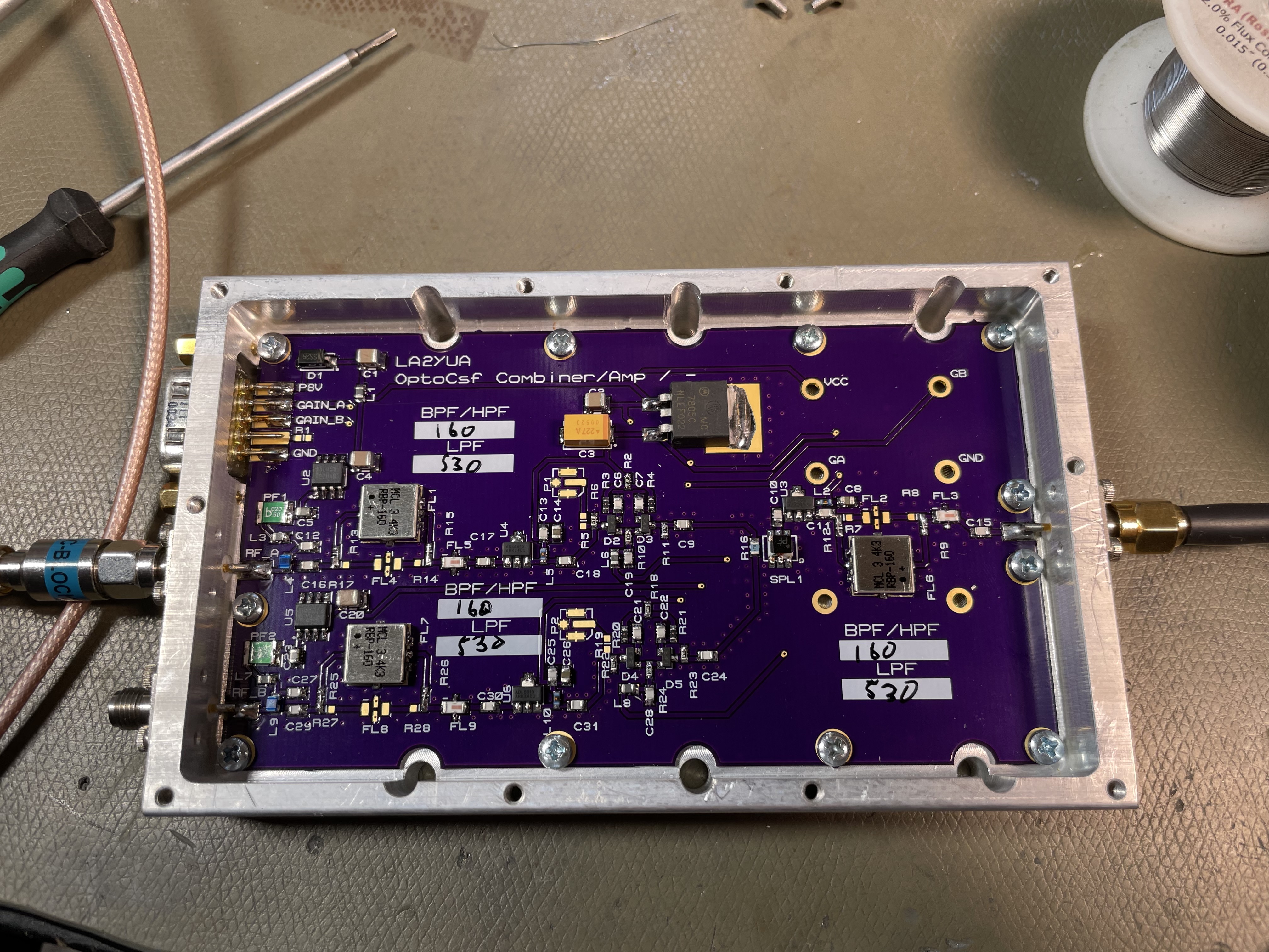
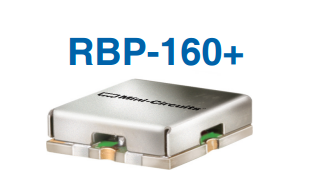
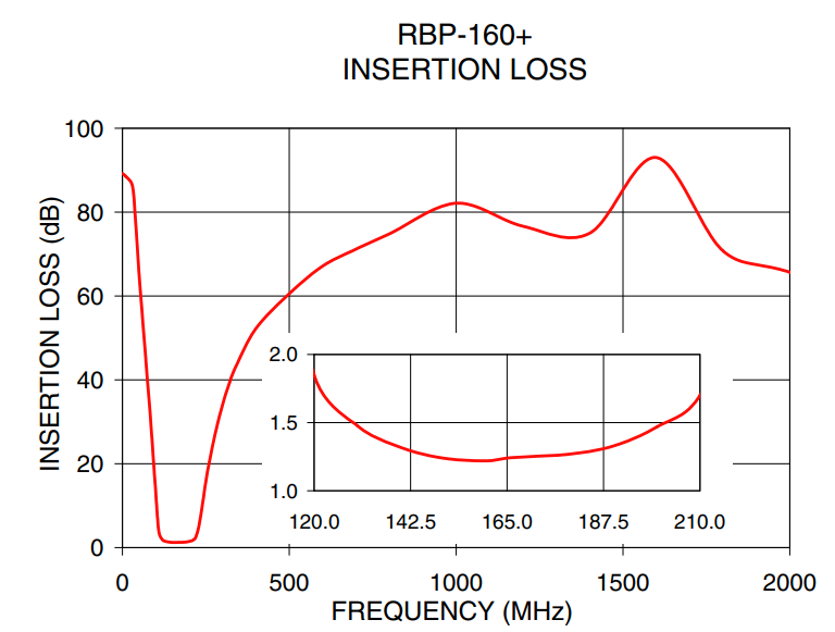
Seen above is the dual VHF input combiner amplifier, this uses the RBP-160 band pass filter on the inputs/outputs, additionally a LTCC 530 MHz low pass filter is added in series to give more wide band attenuation.
The selected RF amplifier for all functions in this system is the ADL5610, which was selected for its wide frequency range and flat gain vs. frequency. The noise figure of 2.2 dB is sufficient, and the gain of 18 dB is acceptable but not too high.
The primary downside of this amplifier is the relatively high current consumption, adding up to around 400 mA per unit if the antenna preamplifiers are included.
The use of a linear 7805 regulator to drop the 14 V input to 5 V doesn't help, but I was too scared to put a switching regulator inside the RF enclosures. A future upgrade could be to add an external switching 8 V regulator to power the amplifier boards, this would roughly halve the losses in these boards.
A few plated holes near the top right are included to allow installation of an AGC/gate board in future, but at the time of writing this has not been implemented on any band.
It is likely that an inline gating module will be added to the VHF/UHF ranges to disable the channel if the input power exceeds some threshold, which is usually the case when a local transmitter is active.
Filter Sets
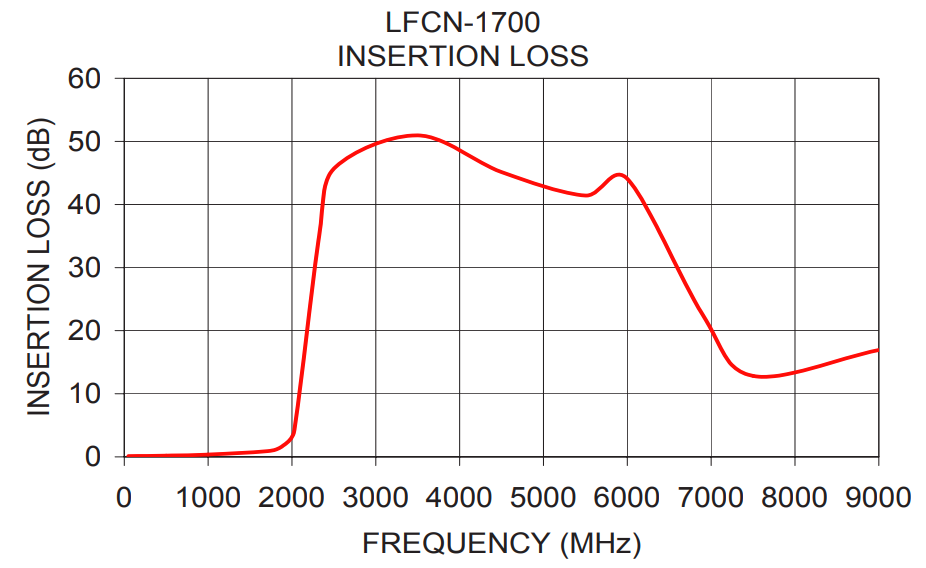
I used Mini-Circuits filter modules for the filtering in the combiner/amplifier modules, for lower frequencies I selected the RBP module series, and for higher frequencies LTCC ceramic filters are used.
The RBP filters in particular are relatively expensive, but offer very good performance. As mentioned above, I used LTCC low pass filters in series with these filters to extend the usable stop band performance.
The filter sets selected are:
- 2⨉RBP-160+LFCN-530
- 2⨉RBP-400+LFCN-530
- HFCN-1000/LFCN-1000 for 1090 MHz
- HFCN-1000/LFCN-1000 for 23 cm
- 2⨉HFCN-1000/LFCN-1700 for L-Band
Note that the antenna preamplifiers typically have narrower frequency responses than these filters.


Link Budgeting
The selected laser in this case is an Ortel 1540B series device, which is a high power laser with included RF port, and it is already specified as an RF component!
The laser diode is an extremely insensitive device, but at least we now know some typical figures:
We see that a typical noise figure in our range is around 45 dB in our case. This is significant, and a lot of gain is required to drive this with optimal noise. Note also the extremely wide bandwidth of the laser, this could be useful in the future! (Not in this article though.)
The IIP3 is relatively high in absolute terms, but relative to the noise figure this isn't very high either.
Using AppCAD a preamplifier module was specified to match the laser and handle the bulk of the gain required in the system.
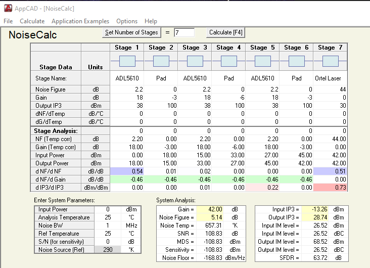
By using 3 pcs ADL5610 LNAs in series, with a few pads in between, a total system gain of 42 dB was found to be most practical, yielding a noise figure of around 5 dB for the combined laser and preamplifier.
The use of attenuators serves both to prevent overloading the cascaded amplifiers, and also to limit the LNA output power to a safe level for the laser.
The total dynamic range is over 100 dB for narrow band signals, and the spurious free dynamic range is around 60 dB.
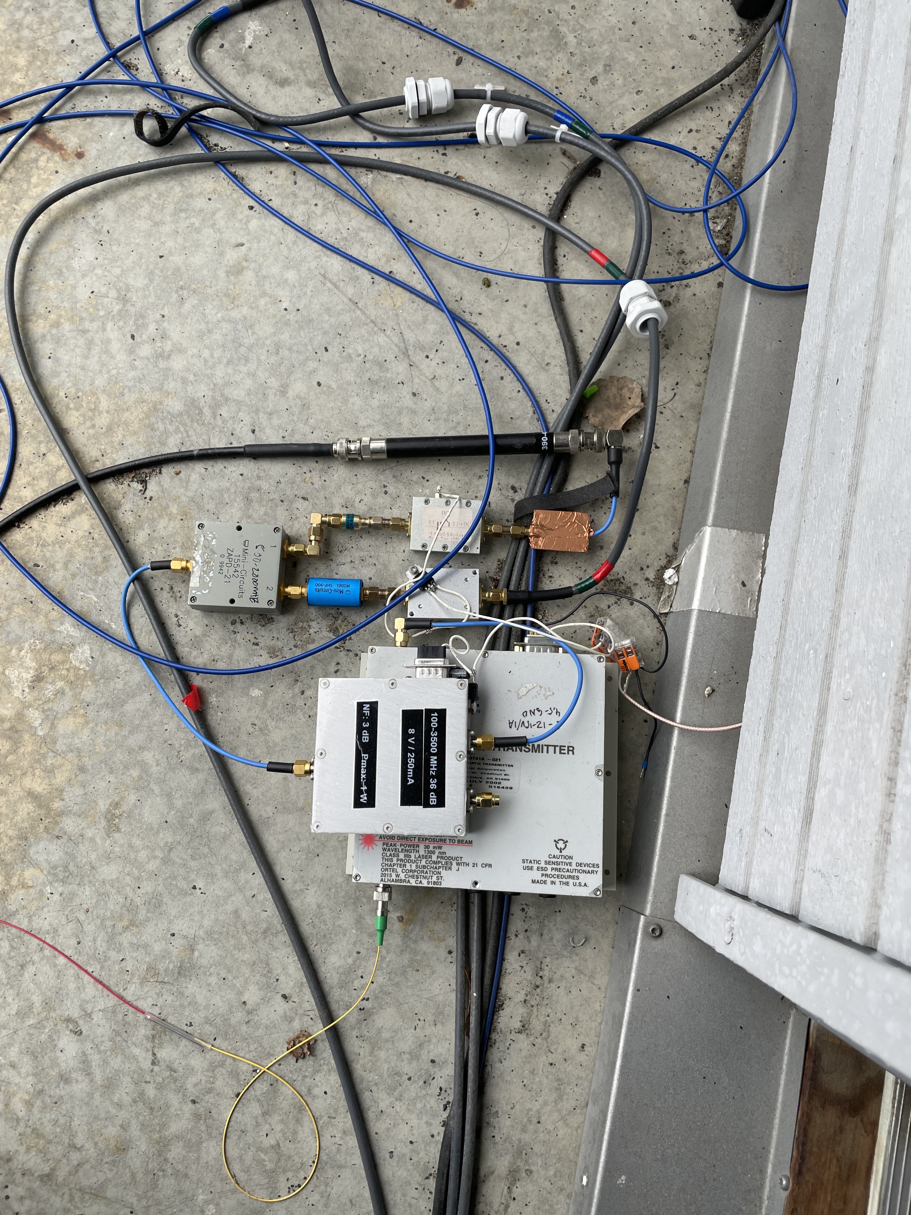
Laser Preamplifier
The laser preamplifier described above was the first completed module in the system, being done months in advance of the rest of the system. It was also used in the risk reduction testing phase.
The laser preamp was built in another repurposed shielded enclosure, it implements the above amplifier chain with 3 pcs ADL5610 + intermediate pads. Since the enclosure had 3 RF ports I put in an output splitter, allowing the laser drive signal to be tapped off if desired.

The black things are conductive RF foam contacting the chassis lid, this prevents some undesired case resonances in the 2-3 GHz range.
The amplifier is good to 3 GHz, which is also reinforced by a LFCN-3000 low pass filter on the input/output to reduce the noise bandwidth. This was done in case I want to use even higher signal frequencies later, these would require a new laser preamplifier anyway. In this case a new combiner would be inserted between the laser preamp and laser.
The amplifier unfortunately runs off 8 V DC instead of 14 V DC, the decision to use 14 V for the remaining system was made later (mainly because of the PIN attenuators), so a 7808 regulator is bolted to the outside of the amplifier chassis (not shown). This amplifier uses low noise voltage regulators, one per LNA, which is not required but seemed to make sense.
A RLM-33+ RF limiter was added to the input to prevent damage, making this a fairly robust module.
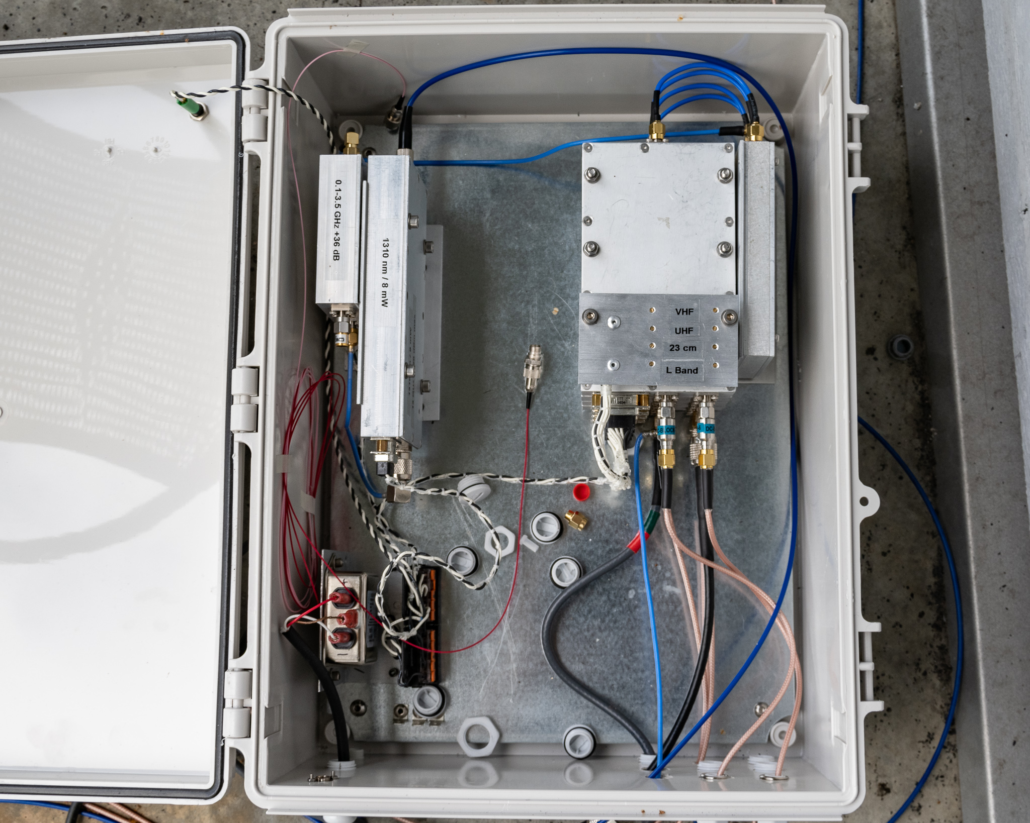
Laser Module
Two different laser modules were built as part of this project, both using very similar Ortel 1540 series lasers. These are both 1310 nm, though there is little practical difference between 1310 and 1550 nm for this use case.
The 1540 series lasers are very high quality devices, and offer around 10 mW output power, and good spectral purity., These units are thermally controlled using a thermoelectric cooler (TEC).
Above the block diagram is shown for the laser itself, showing the various components included.
Above is a picture of the large "lab" version of the laser module, this version is housed in the original Ortel chassis with new control electronics. The lab version adds front panel adjustable power and banana plug power inputs.
The original electronics did not include the front panel power control, required two supply voltages, and had an electronics fault when I got it which meant the laser was running at 40+ mW! Fortunately the laser seems relatively robust at least.
The power control regulator is a modified variant of a previously described analog laser driver; the modification is to increase the available output voltage. The rightmost board is a thermal regulator, which uses a Maxim MAX1968 TEC driver IC and analog regulator loop to regulate the laser temperature for increased stability.
The TEC driver uses a switching regulator module to generate a 5 V supply, while the laser driver board has an 8 V linear regulator.
Incidentally, the key issue with variable temperature lasers is mostly that the modulation sensitivity decreases with temperature. That is, the electrical RF power level you need to apply increases with temperature. The wavelength also changes of course, but this isn't relevant non-WDM systems. In this case, the laser is only specified at 25 °C, with the user expected to implement a TEC driver and servo.
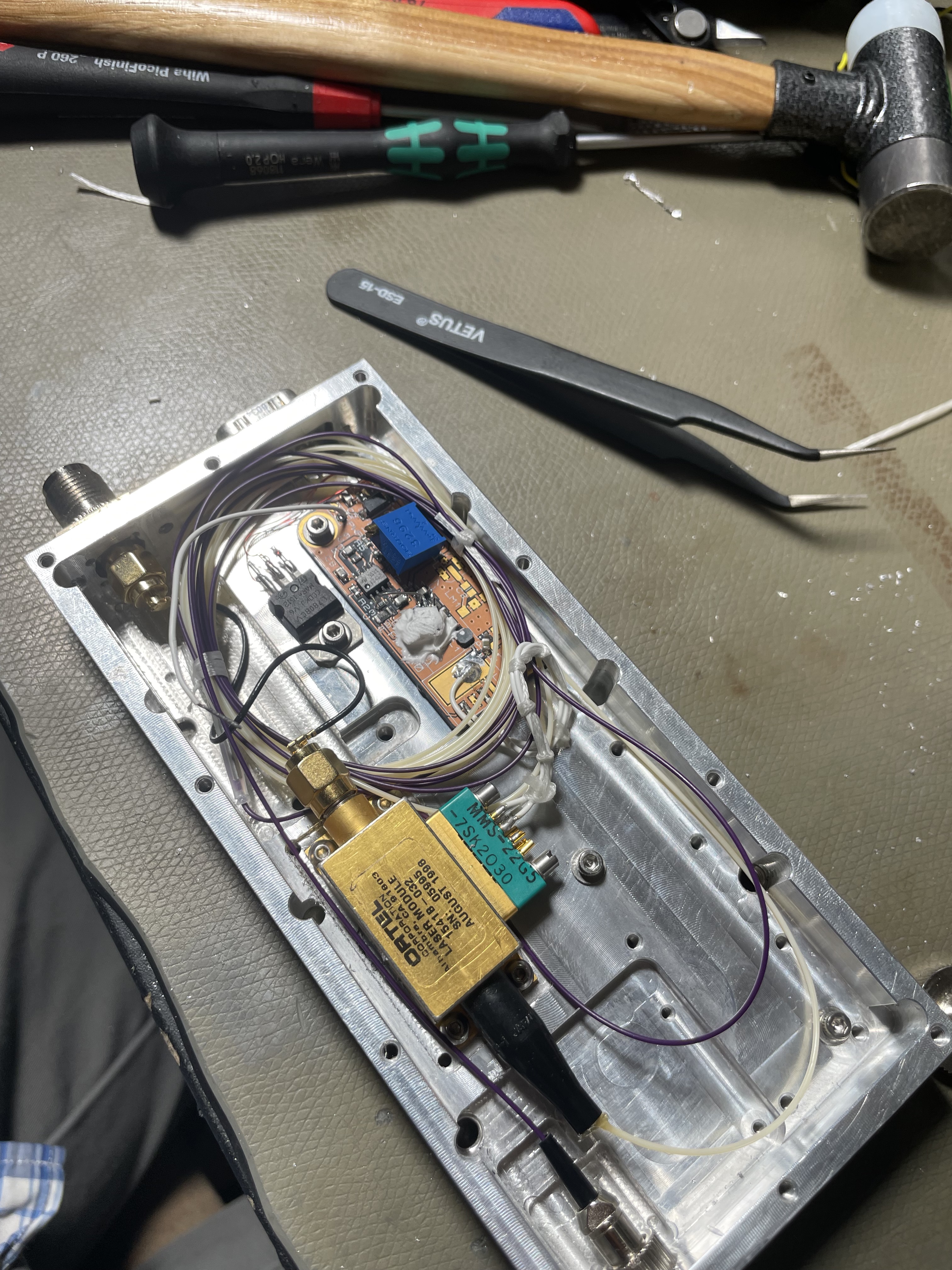
Above we see the final laser module during assembly, but before switching to APC fiber. The TEC module was installed to the top right of the case.
Laser Issues
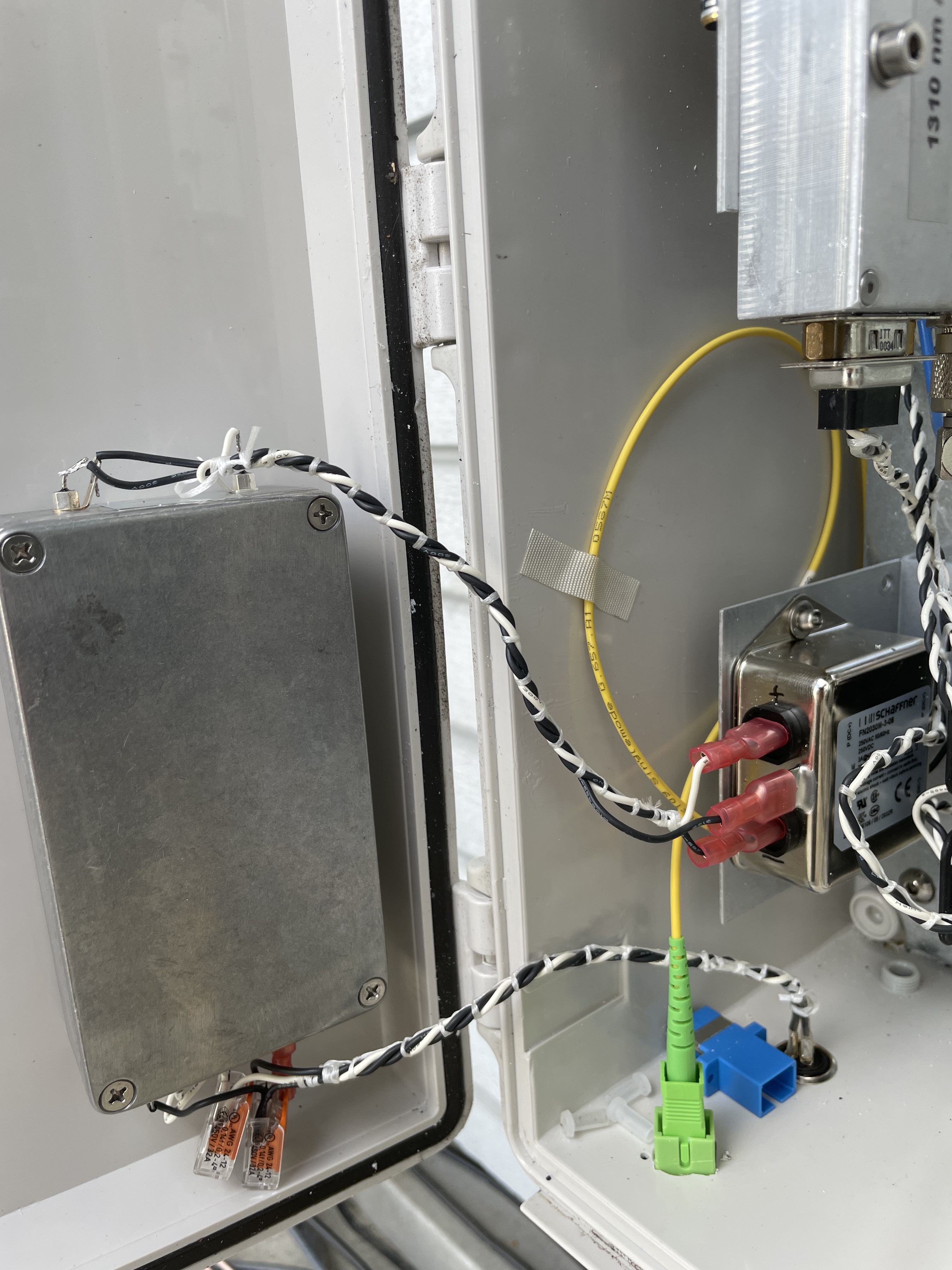
While testing this system I ran into a number of oscillation/noise issues, which turned out to be caused by back-reflections from UPC connectors. I had initially assumed this was a power supply noise issue and was picked up by the antennas in the prototype system.
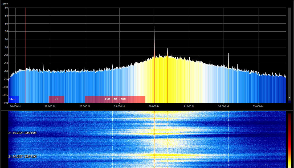
The above behaviour was observed, with multiple harmonics of this chunk of noise. Funnily enough the main issue was that I was using the original "lab" laser before swapping the electronics, and this laser had a UPC output fiber and not APC! I just assumed it had APC, so I was getting around 14 dB return loss to the laser before I even started. I was also running the laser super hard, at least 40 mW (where my meters maxed out) since I was measuring the power through an APC pigtail.
However, I did also have issues after swapping to all-UPC.
In the end this behaviour is laser-dependent, and some lasers have better optical isolators than others. Adjusting the power also helps since it seems that the absolute reflected power matters more than the return loss.
The actual fix is to simply switch all the systems to APC connectors, which has been completed since then, and no similar issues have been encountered. The green connectors are also more æsthetically pleasing 🙂.
Detectors and Distribution
The system is used by several systems as originally intended.
Distribution is handled using PLC splitters, with the high laser power a 1:16 splitter can still be used with passive PIN detectors. However most devices are now connected using active PIN detectors, which were not used with the previous HFoF system.
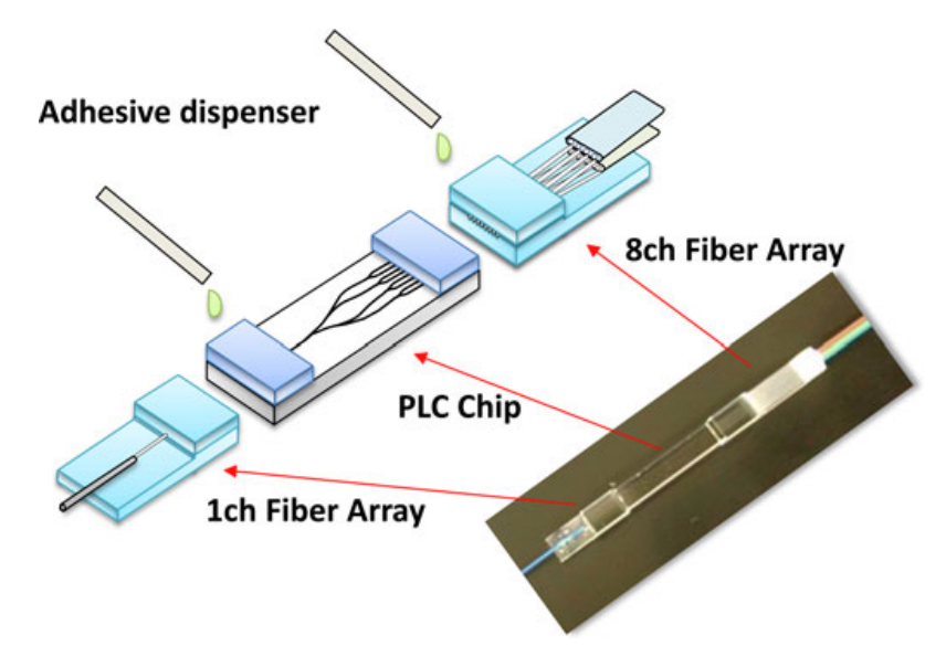
PLC splitters are like magic.
Splitter Losses for RoF Double
It is worth noting that splitter losses are specified in dB, and are measured by optical power.
However, when designing a RoF system we need to double the splitter losses so a 10 dB splitter yields a 20 dB reduction in recovered RF power when link budgeting.
This is not normally notable, since optical systems are generally specified based on optical power and you can ignore the RF levels that result. I didn't pay much attention to this problem either, since I had adjustable gain transmitters and empirical data to design based on.
The issue is that when driving a laser, we convert an RF current into optical power, not an RF power into an optical power.
Upon recovery, the optical power is exchanged into RF current again. If we attenuate the optical power by 10 dB this is equivalent to a 10 dB reduction in RF current, which is the same as attenuating the RF power by 20 dB.
To use a simple calculation, we assume a 1:1 current→power and power→current ratio in the laser and detector (very much not realistic).
Apply 1 mW/0 dBm of 50 Ω RF power, resulting optical power is the RF current, around 4.5 mA (I=√(P/R)) = 4.5 mW.
Apply 10 dB attenuation in the RF domain and we would get -10 dBm (100 µW), corresponding to around 1.4 mA.
However, applying 10 dB optical attenuation and the fun starts:
Optical power reduced from 4.5 mW to 0.45 mW. The resulting RF current is then 0.45 mA. In a 50 Ω system this corresponds to 10 µW, or -20 dBm (by P=I⨉I⨉R) and our 10 dB splitter gave us 20 dB of signal loss.
Designers of RoF distribution beware, here be losses!
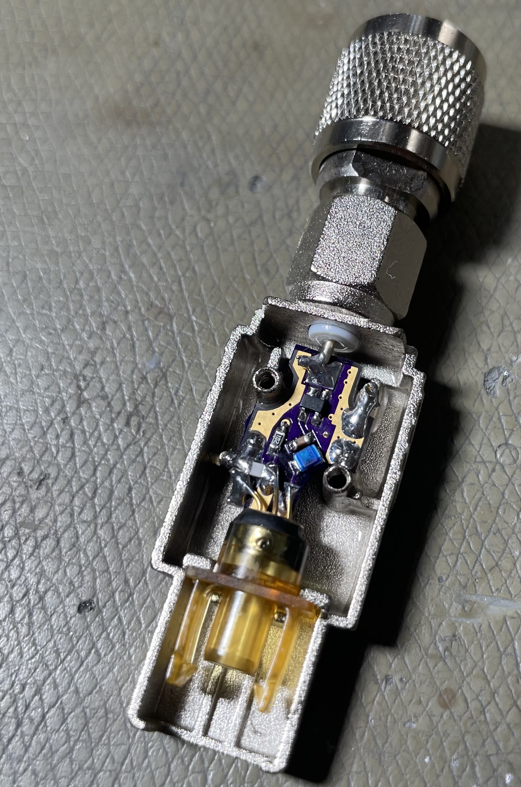
Active PIN Detector for VHF+
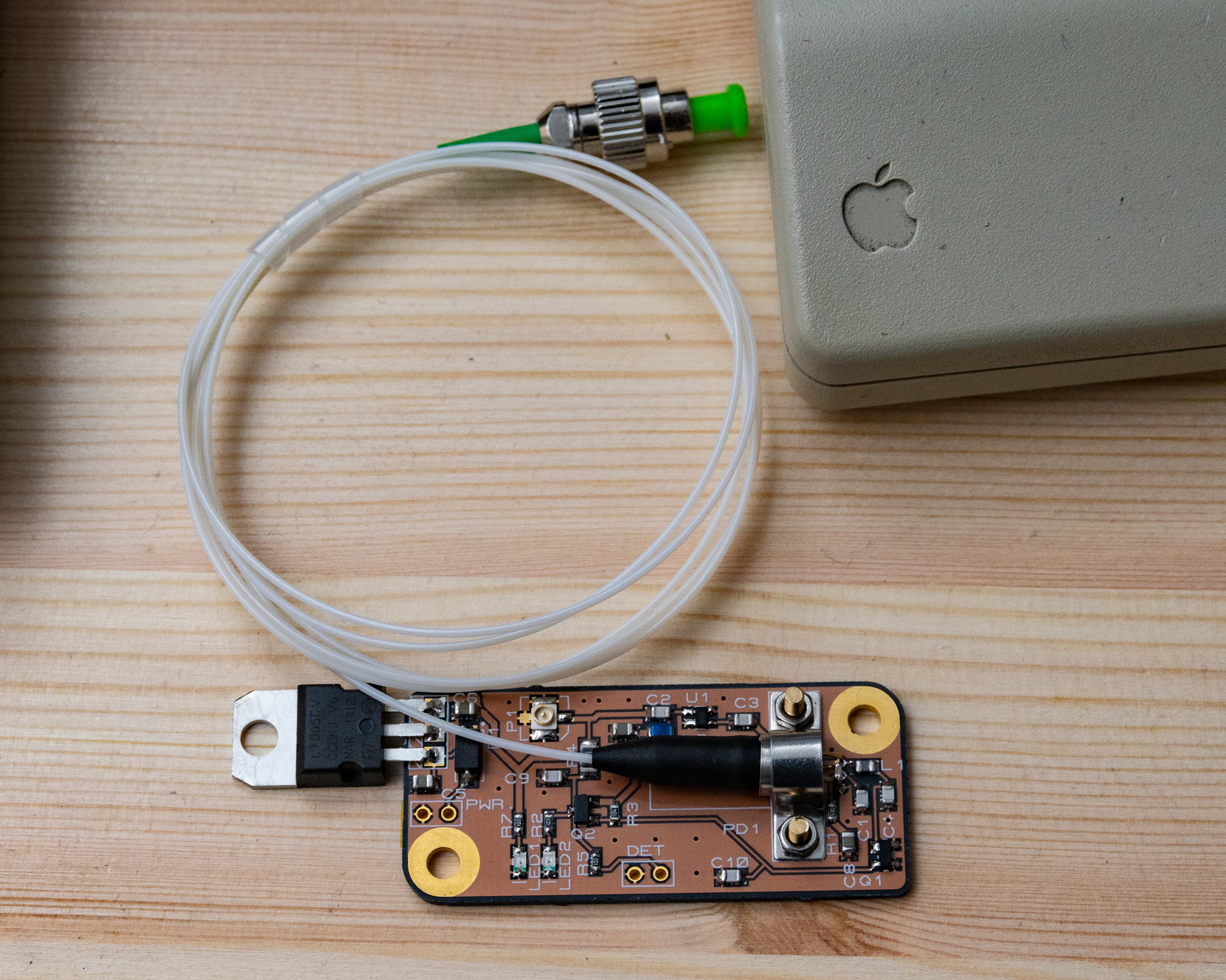
I built a few "large" detectors using the PSA4-5043+, these are housed in die-cast enclosures with feedthrough capacitors for power etc.
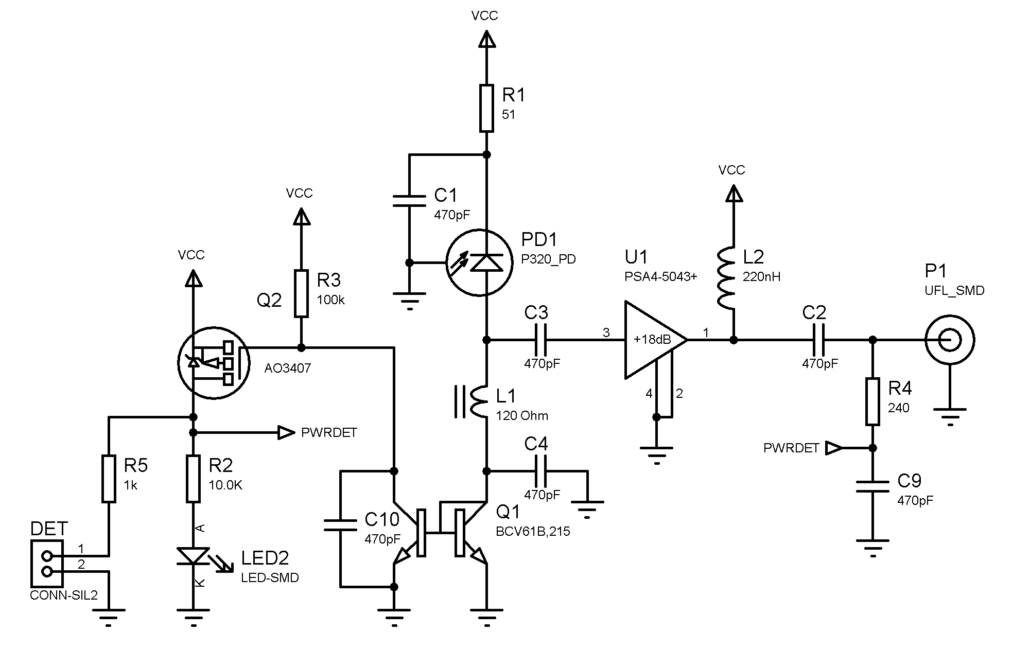
These assemblies use pigtailed InGaAs PIN diodes with external power. The PSA4-5043+ is a very low noise amplifier, but it is not ideal since it has a very wide gain variation vs frequency.
The ADL5610 is better, since it has flatter gain, and the slightly higher noise figure is not of concern since the output noise level of the PIN diode and source signal dominates. This amplifier has been used in some later more integrated designs where the power consumption is not as critical.
Note that Q1 is a current mirror, which senses the diode DC current and drives a LED when an optical signal is connected. RF-wise Q1:C could be grounded and the entire left half of the schematic removed.
Compact Bias-Powered Detector
A compact bias powered detector can be easily built inside an ORH-1201 assembly:
The above detector uses a PSA4-5043+ LNA, which as mentioned above is not ideal, but the low power consumption wins out in this case since many receivers are designed for ~30 mA bias output, and would struggle to drive the ADL5610's ~90 mA.
Above I built a custom PCB to implement this, though I also built 5-6 of these with copper- and kapton-tape, with no notable difference in performance between the two solutions.
Complex Filter-Switched SDR Front End
The PlutoSDR struggles with intermodulation products in the VHF band (it's not specified for this range, and it shows).
To resolve this as well as some other practical issues, I designed a front end board for it.
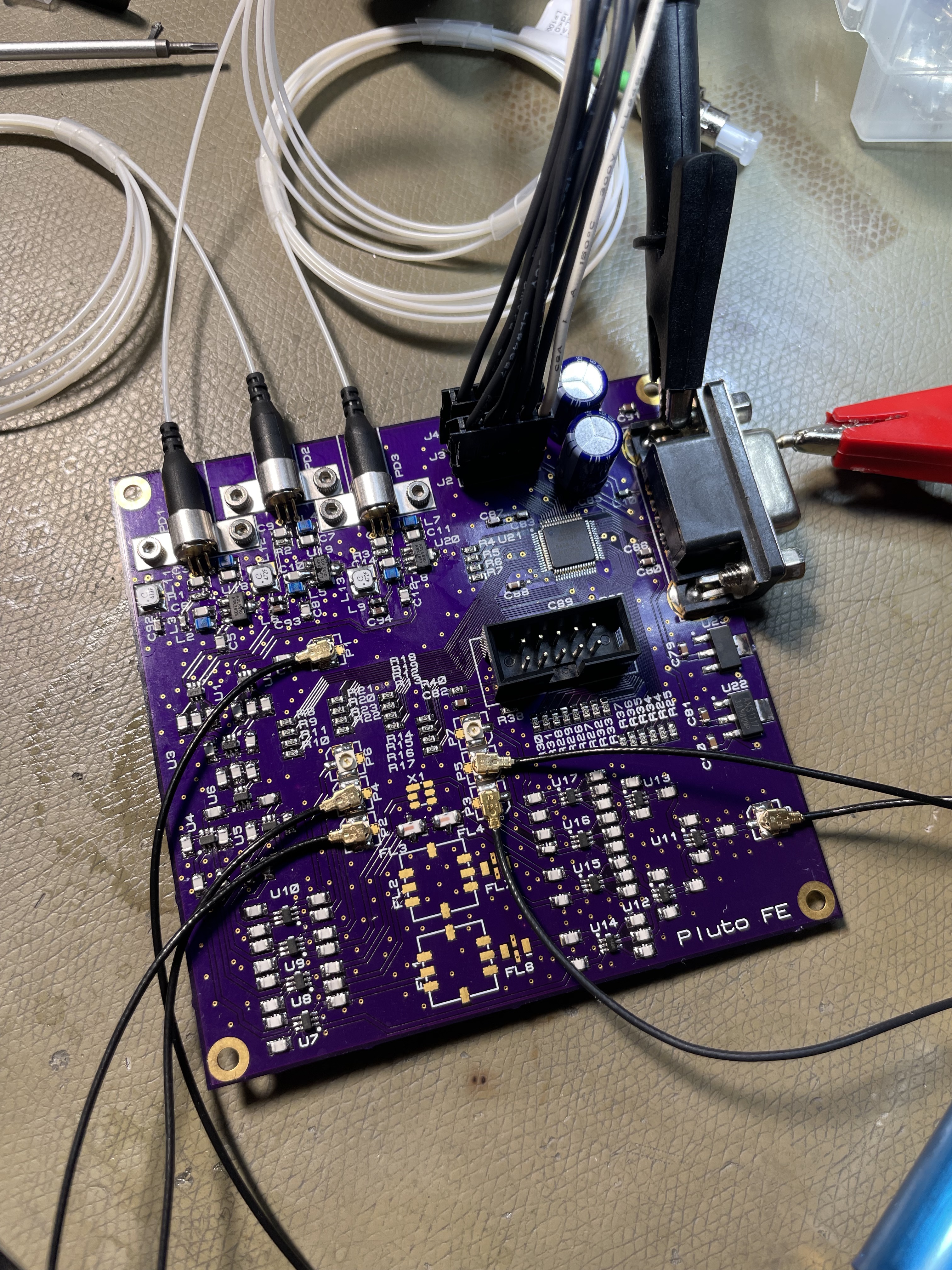
The above assembly has four inputs, three of which are optical. This design uses the ADL5610 preamp to good effect. The PIN diodes are otherwise standard pigtail types.
The multiple inputs are not required at this time, but I expect that e.g. Ku/Ka-band satellite systems may be built in future, and that type of system would realistically require a separate fiber-system, including two-way transmission to transfer a time base for the LNB.
The board also has 8 selectable filters, using the same filters as the fiber system, with some additions such as a 1545 MHz SAW filter. There are also three external filter ports that can be connected to external connectorised filters.
As pictured above the relevant filters had not arrived yet, so only the 1000-1700 MHz + external filters were available.
As clearly seen above, this design required a lot of RF switch ICs, and a CPLD is used to control the switch states based on external switches (in future this will also be remote controlled by the PlutoSDR itself using an SPI interface).
Portable Unit
I had two spare combiner/amplifier PCBs and enclosures that were also assembled with wider filter bandwidths for experimental use. One of those was assembled in a plastic waterproof enclosure.
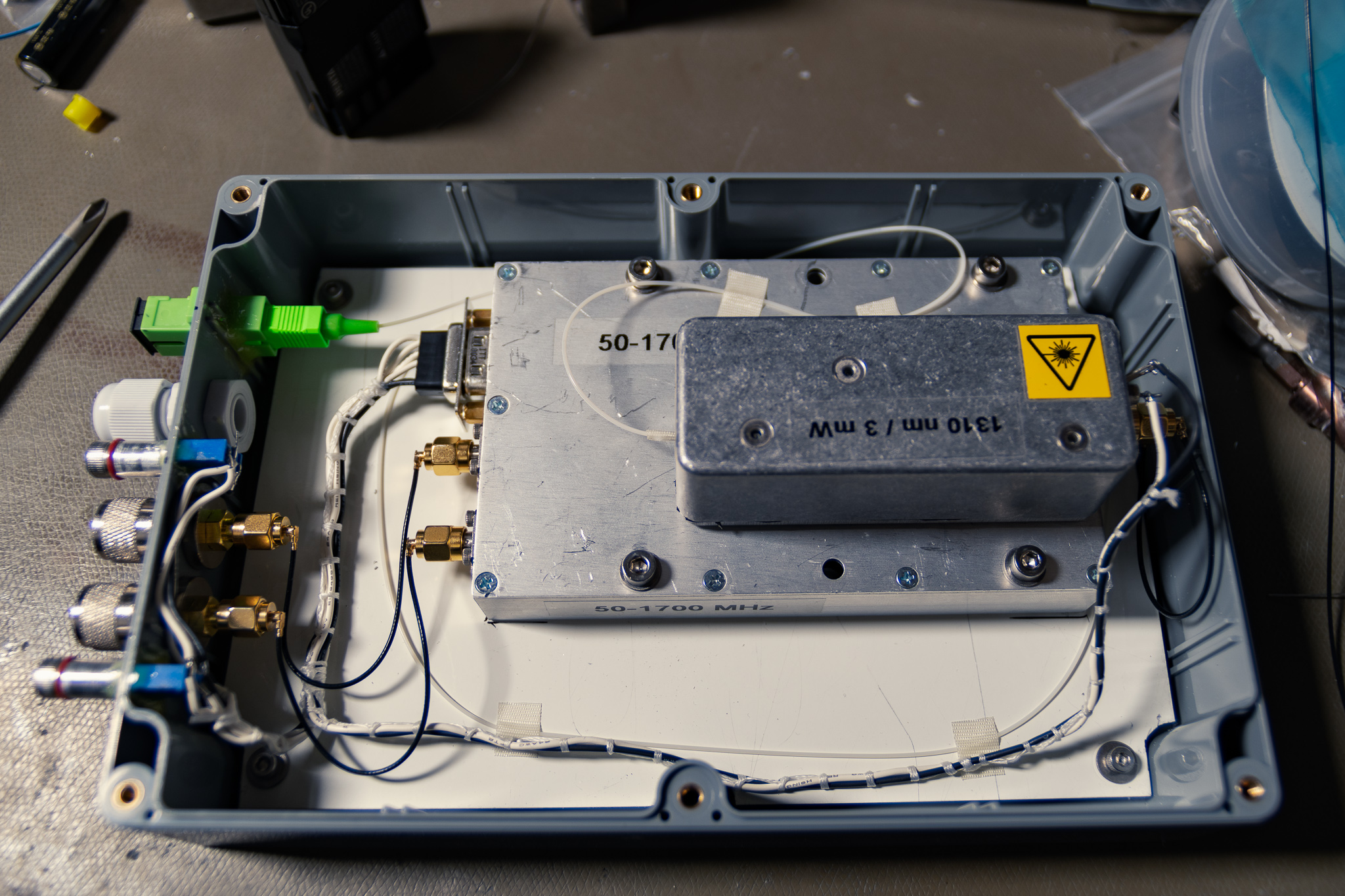

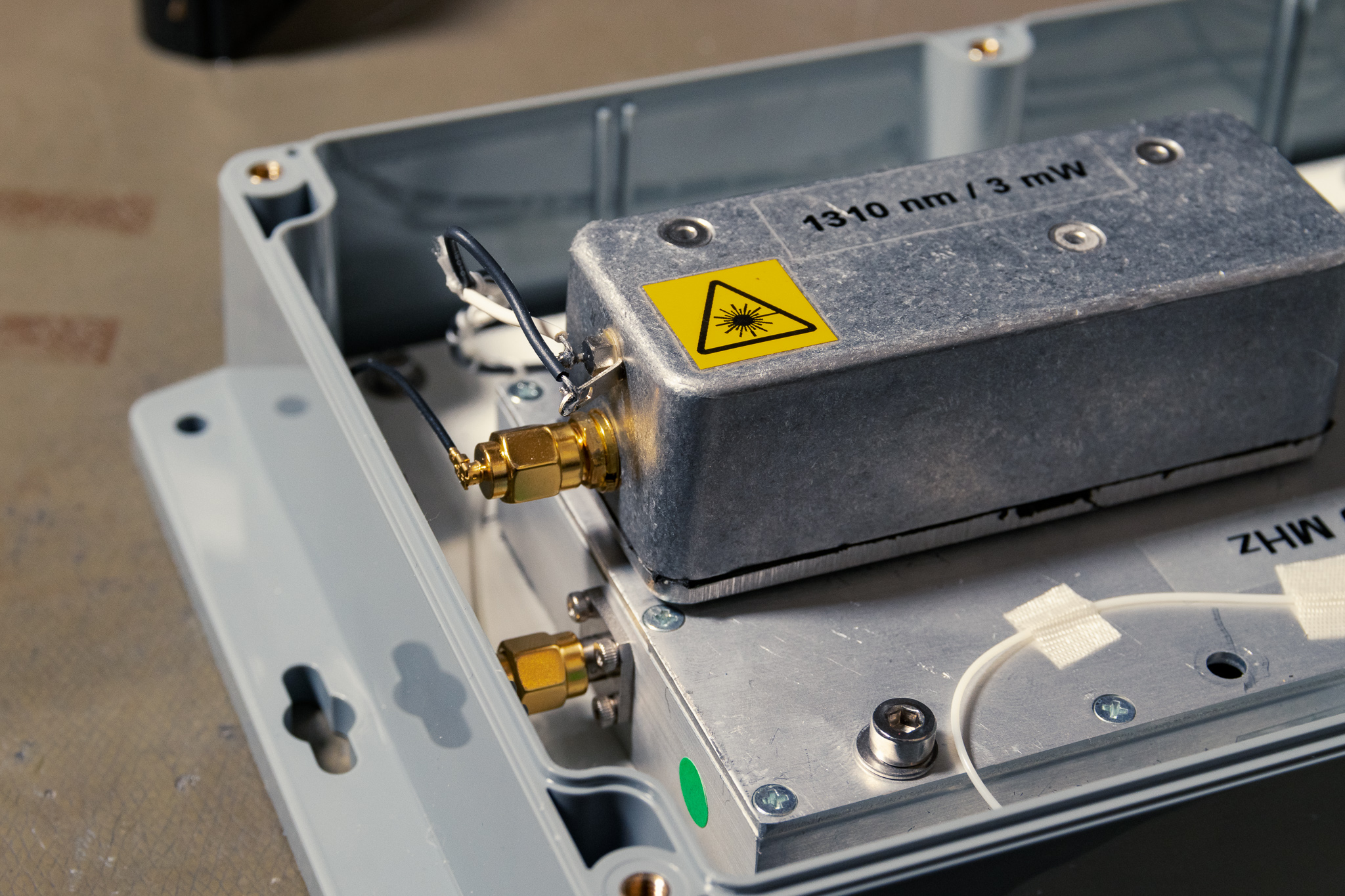


This assembly is wide-band on both channels, and can be used for test setups or demo use. It does not include the additional laser preamplifier module so a high gain antenna preamp is required for proper use. A basic uncooled 3 mW FP laser is used instead of the higher performance cooled DFB laser.
Gain control is via two potentiometers as before.
SDR Distribution
To feed SDRs (for e.g. D1090, VDL2, Radiosondes,) I simply use one of the active detectors above, which is hooked up directly to several band pass filters (no splitter, just T-joints). Since the amplified detector output levels are so high, the losses incurred are not significant to system performance.
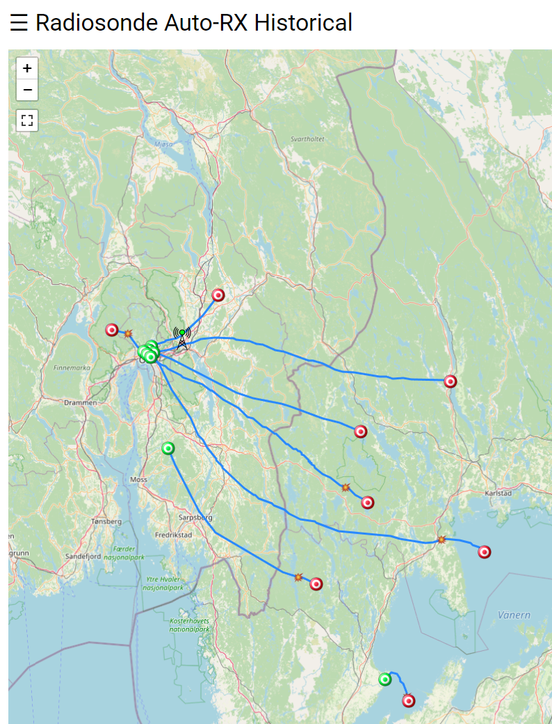
The RTL-SDR stack is in itself a project, and may warrant its own article.
While a RTL-SDR can for the most part handle being directly hooked up to this system, I have found performance to be slightly better when used with dedicated band pass filters per SDR.
Antennas
A variety of antennas are used with this system, though this is always evolving.
- Sirio GP 108-136 LB/U 1/4 λ GP with basic filtered preamp
- Since we don't have much FM broadcast, the need for filtering is limited
- Later replaced with a RBP-160 preamp
- 150 MHz 1/4 λ whip for DAB with AliExpress DAB BPF & LNA
- This is kind of superflous and may be replaced with something more sensible later
- Later decommissioned, since DAB harmonics affected the 430 MHz range
- 406 MHz 1/4 λ whip for Radiosondes, with custom RF3607D SAW filtered LNA
- We have a lot of TETRA around 390 MHz so SAW is basically required
- The RF3607D filter covers ~395-415 MHz
- Sirio GP 430 LB/N 1/4 λ GP with modified AliExpress SAW LNA
- The SAW filter covers ~420-450 MHz with low loss, modified to put the SAW filter in front of the LNA due to intermod issues
- PCB LPDA 600-6000 MHz for 1090 & 1200 MHz
- Modified GSM-R interdigital filters with coax diplexer and separate LNA's, ~1.5 dB NF
- AeroAntenna AT1675-381 Survey Antenna for GNSS & L-Band services
- I point it south to cover geosats, it still picks up GNSS just fine!
- Tallysman Active Iridium PNT puck antenna
- This is not too useful so may be replaced
- Routed through an interdigital filter since the preamp on this one has a wide noise bandwidth that interfered with GPS L1
Conclusion
The Radio over Fiber system implemented offers acceptable performance and extreme convenience compared to an equivalent coaxial distribution system.
Performance is limited by the antenna/preamp combination, and devices such as GNSS receivers perform extremely well when connected with one of the active detectors described above. Connecting a new receiver to the system will never degrade the performance of existing receivers in any way.
The downside is that strong interference in one band does cause dropouts in other bands, though this is almost entirely under my control since no other local transmitter are around. I expect to solve this at a later time by adding overload-gating to the relevant antennas (at the time of writing the PCBs have been ordered).
A significant to some downside is power, the system requires around 20 W continuously, which is significant especially if operating on batteries.
Let's not even talk about the cost (it's less than it might seem, anyway).
The wide bandwidth can be an issue for some receivers, especially SDR receivers without preselection filters. This is usually solvable by adding the relevant filter, though these filters aren't always cheap or plentiful.