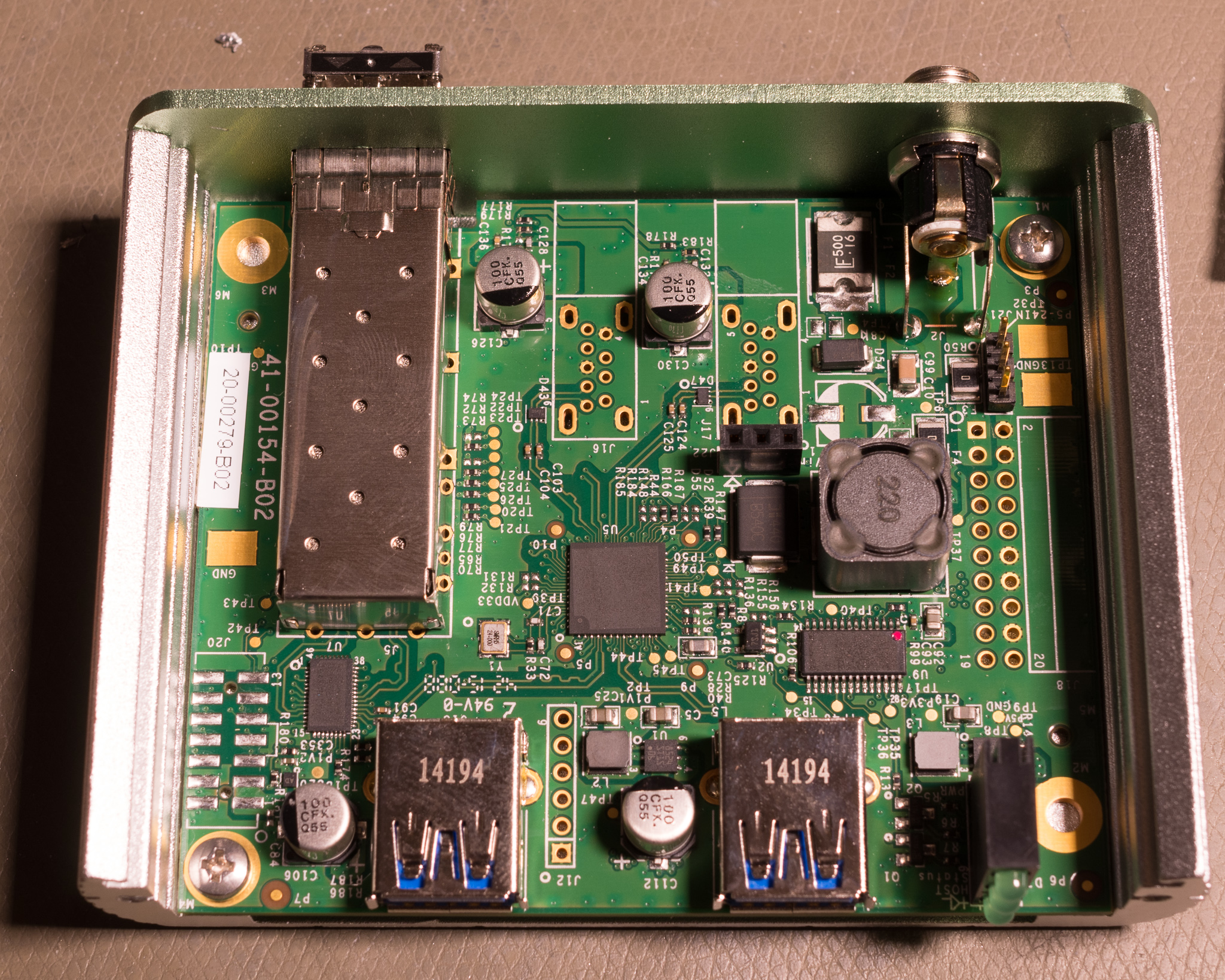
Icron Spectra™ 3022 USB 3.0 Extender REX Teardown
Around the same time that I bought the USB 2.0 extender featured previously I bought some cheap remote units for the 3022 USB 3.0 (5 Gbit⁄s) system.
My thought was that maybe these were identical like the USB 2.0 extender.
From the looks of it I was wrong there and will need to find a LEX to use it, but it was still interesting.
The 3022 is a USB 3.0 only extender, USB 2.0 will not work at all (don't even bother trying it, the ports don't even have the USB 2.0 data pins wired).
As it turns out, USB 3.0 is actually a hell of a lot simpler to extend than USB 2.0 since it uses two unidirectional diff lines instead of a single bidirectional one. This makes it possible to in principle wire this directly to an active extender cable or optical transceiver. It looks like this is what they did for this model. This also means no special ASICs are required — in principle at least.
Power input is listed as 24 V in the manual but mine was marked 5 V (no current given), the board has markings that indicate 5-24 V is acceptable but there is a jumper position and such on the board.
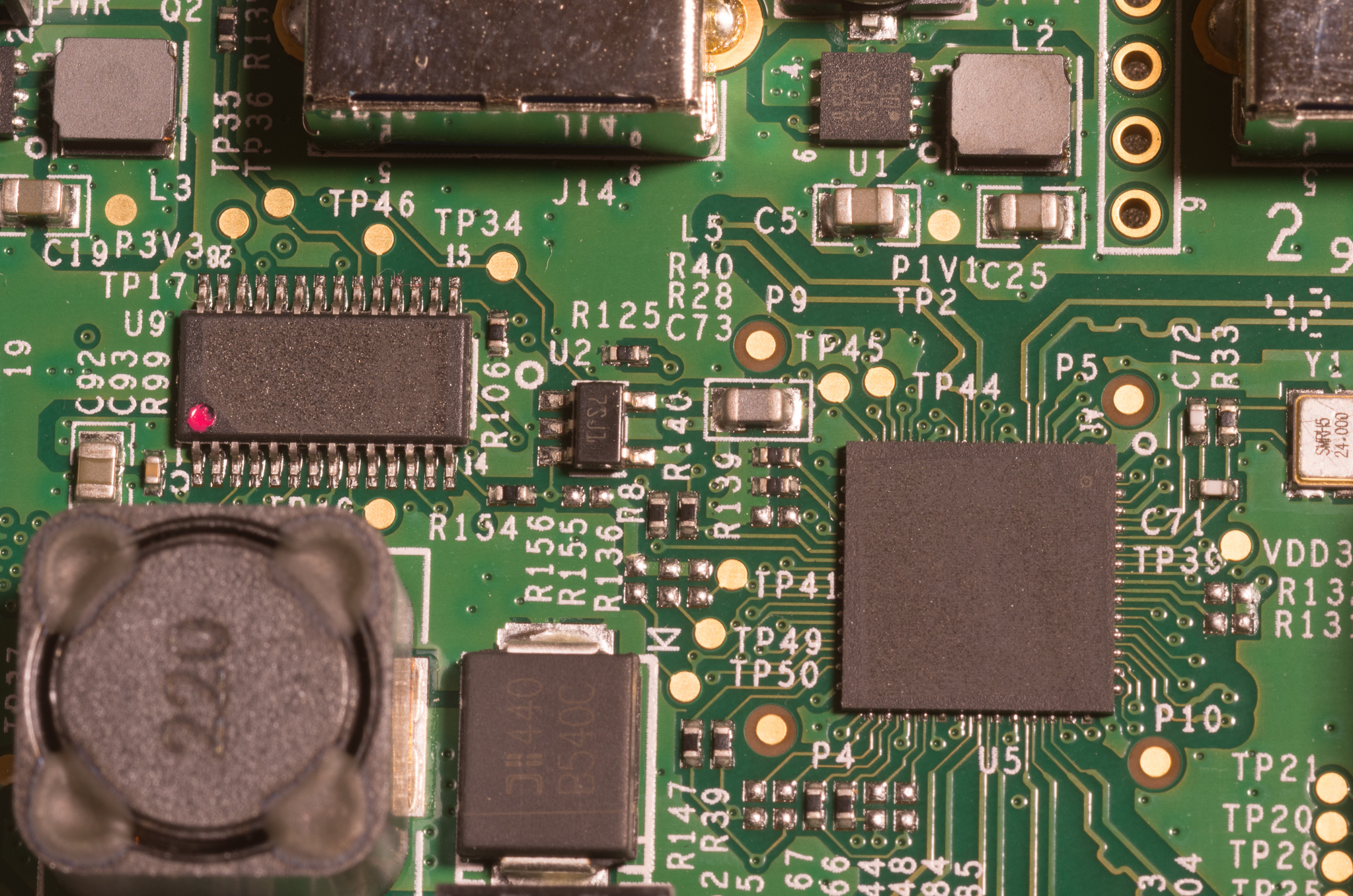
It might be possible to re-configure it to run off either 5 V or a higher voltage. The switching controller is on the bottom and is an ST L7986, rated to 48 V input and 3 A output on its own, suggesting that this is a wide-input design.
I'm assuming this relatively simple solution using off the shelf ICs is why they decided to laser off all the markings on the core ICs. They did a good job too, no trace of the original markings remains.
The SFP+ module is also unbranded, it's probably a 10G ethernet module or an 8G FibreChannel module though, nothing special about that. It looks like a standard Avago module (same design for the latch).
Note that there are three ICs that are lasered, the rest is power and basic logic gates.
Also note two USB 3.0 type A footprints near the back that are routed to the main chip but not populated. This is a standard USB 3.0 type A vertical right angle footprint, not too many types exist but the Molex 0484040003 looks like it would fit.
My initial guesses were (left to right): Level shifter between USB levels and CML for the SFP+, USB 3.0 hub (4-port), MCU.
You might think lasering off the markings would make this nearly impossible to figure out, but these ICs weren't too difficult to figure out for various reasons. The biggest uncertainty is the MCU, there are a lot of options but the true test would be to connect a debugger to check the part number.
What Hub is it?
I expected this device to use the same USB 3.0 hub as the Ranger extender, a Cypress something or other. However, that theory is gone as soon as you notice it uses a 24 MHz clock. The Cypress ICs all use 26 MHz clocks.
Microchip and TI make hubs with 24 MHz clocks.
Next step is to narrow things down by looking at the pinout, at first glance it looks like a standard QFN with 52 pins (13 on each side), but look closely at the traces and you'll notice something is fucky here. Half the traces seem to come from further back under the package. Also, there's no common 52 pin QFN package.
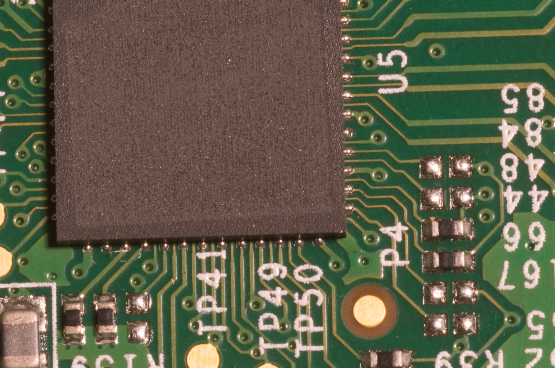
Assuming it's a 25x25 package that's a more standard QFN-100, but it's actually a pretty unusual staggered pin QFN. Using the Digi-Key search it was quick to narrow it down to a TI TUSB8040A.
The TUSB8040A provides simultaneous SuperSpeed USB and high-speed or full-speed connections on the upstream port and provides SuperSpeed USB, high-speed, full-speed, or low-speed connections on the downstream ports. When the upstream port is connected to an electrical environment that only supports high-speed, full-speed or low-speed connections, SuperSpeed USB connectivity is disabled on the downstream ports. When the upstream port is connected to an electrical environment that only supports full-speed or low-speed connections, SuperSpeed USB and high-speed connectivity are disabled on the downstream ports.
Regarding the spare ports:
The TUSB8040A supports up to four downstream ports. It may be configured to report one to four downstream ports by pin selection or by an attached EEPROM or SMBus controller. The configuration options provide the ability to scale the device by application.
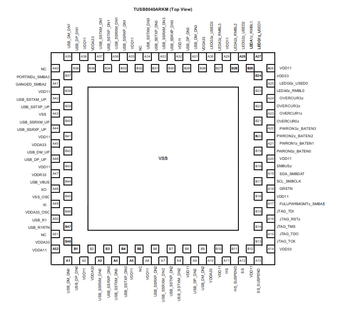
This is as expected a 4-port USB 3.0 hub IC, they have broken out two of the ports on the front and left the rear ports unpopulated (with no mention of there existing a 4-port model at all). I would have expected them to disable the spare ports by default, but at the end of this post I recorded the hub config sequence and it looks like these are enabled and will probably work if connected.
MCU?
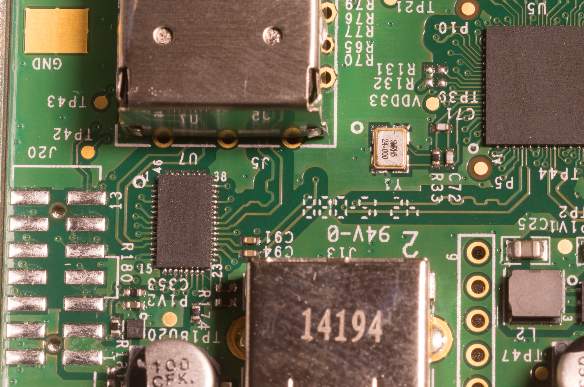
The MCU can be seen below, it is a TSSOP 28 pin package, the paint dot likely indicates it was pre-programmed before installation. My best guess is it's a TI MSP430G2x33 or something very similar.
Out of the available MCUs in this package the MSP430 is by far the most commonly used type. There actually aren't that many different MCUs in this package to choose from.
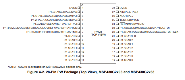
The exact type is not super important unless someone wants to dump and modify the source code (or just re-write it from scratch, it's probably pretty simple code.)
Level Shifter
There is a final strange IC near the SFP+ module:
It's plainly obvious that this IC is connected between the hub host side ports and the SFP module, so I assumed it was some kind of driver-IC. The package is a quite uncommon 46-lead QFN. This information alone was enough to narrow it down to some kind of Renesas line-driver for high speed applications.
After looking over the 4 different options Renesas offers I believe it's a QLX4600:
The QLx4600-SL30 is a settable quad receive-side equalizer with extended functionality for advanced protocols operating with line rates up to 6.25Gb/s such as 4k video capable DisplayPort v1.2 (HBR1/2), InfiniBand (SDR and DDR) and 10GBase-CX4. The QLx4600-SL30 compensates for the frequency dependent attenuation of copper twin-axial cables, extending the signal reach up to 30m on 24AWG cable.
The small form factor, highly-integrated quad design is ideal for high-density data transmission applications including active copper cable assemblies. The four equalizing filters within the QLx4600-SL30 can each be set to one of 32 compensation levels, providing optimal signal fidelity for a given media and length. The compensation level for each filter can be set by either (a) three external control pins or (b) a serial bus interface. When the external control pins are used, 18 of the 32 boost levels are available for each channel. If the serial bus is used, all 32 compensation levels are available.
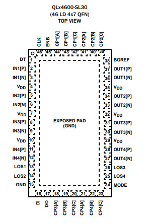
The pinout is a match, and the line rate is around 6 Gbit⁄s for this IC which is sufficient for 5 Gbit⁄s USB 3.0 Gen 1.
So basically this IC is used to re-drive the signal between the USB Hub and the SFP+ module. It seems like this wouldn't be necessary for such a small board with short traces.
Summary - The spare ports
The device seems reasonable, it will be interesting to attempt to make the two additional ports work if I find a reasonably priced LEX later.
The type A connectors should take either a Molex 0484040003 or a Stewart SS-52000-002, and it looks like all other USB and power related components are already fitted for these ports.
I²C Bus Sniffing
The I2C bus was relatively easy to find, R139 and R140 are the pullups right by the hub IC. The Hub and SFP+ module are the two devices I saw active on the ²bus.
I did some sniffing of a normal power-up sequence:
Enter Config mode:
- Write 0x40, 0xF8, 0x02
- Register F8 - Set SMBus Reset
- Write 0x40 0xF8
- Setup read reg F8
- Read 0x40
- Read 0x01 - cfgActive asserted
Setup device:
- Write sequential 0x40 addr 0x01:
- 0x00 - Vendor ID LSB
- 0x00 - Vendor ID MSB
- 0x00 - Product ID LSB
- 0x00 - Product ID MSB
- 0x24 - Device Config Register
- Set register 5 bit 5 and bit 3: "u1u2Disable" and "ganged", clear all others
- 0x00 - Battery Charging Support
- No battery charging support
- 0x00 - Device Removable
- All ports reported as non-removable
- 0x0F - Port Used Configuration
- Set register 0x08 lower nibble - enables all 4 ports
- Write 0x40 0xF8 0x01 - Exit SMBus Configuration Mode and allow normal hub operation
These SFP+ reads are based on the Finisar spec for DDM modules; it might be inacurate. Registers for SFP modules are in decimal instead of hex per convention.
- Write 0x51 0x60
- Setup read of SFP+ DDM registers, bank 2 at offset 0x60 (96)
- Read 0x51:
- 96 0x16
- 97 0x1C
- Temperature monitor LSB+MSB - around 22 degrees
- 98 0x81
- 99 0xEF
- VCC
- 100 0x00
- 101 0x00
- TX Bias Current
- 102 0x00
- 103 0x00
- TX Power
- 104 0x00
- 105 0x14
- RX Power
- 106 0x00
- 107 0x00
- Reserved
- 108 0x00
- 109 0x00
- Reserved
- 110 0x82 - Control Line Status
- TX Disable Set, TX Fault Set (probably linked to disable)
- 111 0x00
- Reserved
- 112 0x05 - Alarm Register
- TX Power Low Alarm, TX Bias Low Alarm
- 113 0x40 - Reserved Alarm
- Unknown alarm
- 114 0x00
- Reserved
- 115 0x00
- Reserved
- 116 0x05 - Warning Register
- TX Power Low Warning, TX Bias Low Warning
- 117 0x40 - Warning Register 2: Warninger
- RX Power Low Warning
- 118 0x00
- Reserved
- 119 0x00
- Reserved
Based on this I conclude for now:
- The Hub will probably work if you fit the additional type A ports
- The SFP module is equipped with DDM and the REX is a slave device that only enables its transmitter when it gets a signal
- There is no explicit check of the module type, but DDM seems to be required
There does not seem to be any continuous readout of the SFP+ DDM info, so I assume the MCU uses the discrete status and control lines to determine if a signal is present. DDM info is probably read periodically when it has a link.