Meinberg PZF180PEX

The Meinberg PZF180PEX is a fairly uncommon sight in northern Europe. It is a PCIe radio clock receiver for the German DCF77 long wave time signal, made by German company Meinberg.
Table of Contents
DCF77
While you can get many a cheap receiver for the DCF77 signal, this card is special due to its use of the special spread spectrum modulation overlaid on the time signal. This signal is similar to a GPS signal in that a correlation receiver can perform a correlation on the received signal to more accurately determine the time of arrival. This method of detection is also less sensitive to noise, and allows tracking with lower SNRs than the standard amplitude based method.
A receiver like this can achieve around ±50 µs precision on the 1 PPS clock phase, assuming you "calibrate" it by telling it the distance to the transmitter. This is actually quite good, since most receivers for DCF77 can only do a few ms accuracy. This also makes DCF77 a much more attractive signal than MSF60 for a precision timing system, since MSF does not provide this additional feature. Unlike GPS the 1 PPS phase offset can't be automatically calculated since these signals are not positioning signals.
TDF162 is another interesting system which may have to be covered in a future post (for now, here's a GitHub repo). The only viable receiver project I've seen was this French design, but the signal is apparently so widely used in France that it's become largely impossible to turn off any time soon. Simulations of recorded data indicates a coherent correlation receiver will be able to track this signal reasonably well at my location.
The frequency precision is not specified anywhere I could see it, after an initial settling period it appeared to stay within 0.1 Hz of my GPSDO on the 10 MHz output which is certainly acceptable. With a long averaging time and a stable local oscillator the frequency accuracy of a clock like this can be extremely good, though I would expect it to drift a bit up and down as the time of flight to the transmitter site varies.
Why?
Now why would you bother with some late 1950s radio clock system when you have a choice of four glorious GNSS systems according to your political allegiance? Redundancy, and common cause failures. While I do plan on adding another GNSS receiver clock to cover GLONASS and Galileo (NavStar and Beidou already being covered by an existing setup), diversity is desired, and required.
Within my budget multi band timing receivers are simply not an option, so everything GNSS relies on a single fairly narrow easily denied frequency range. It also relies on a single antenna system in my case, but that's not always the case.
The DCF77 signal is much harder to jam over a wide area, and still provides acceptable performance. If LORAN or OMEGA were still on the air I would probably be making clocks to use them as well, adding another redundant source.
The Card
The card a neat low profile PCIe 1x device, and is supported on basically every kind of OS, including all notable Windows versions, as well as Linux/Unices via a GPLed but not mainlined driver.
Construction quality appears quite acceptable, assembled with presumably no-clean flux, mainly built with 0805 passives with some 0603s around, this is clearly not the worlds most modern design. Aside from the BGA packages and PCIe slot this board could feasibly have been built by a dedicated hobbyist.
It occasionally pops up on eBay for around $100-150. Obviously this card is only interesting for European readers, since the range of the DCF signal is "guaranteed" to around 1000 km (though in my experience a good antenna setup can make 2000+ km possible with reduced accuracy and availability).
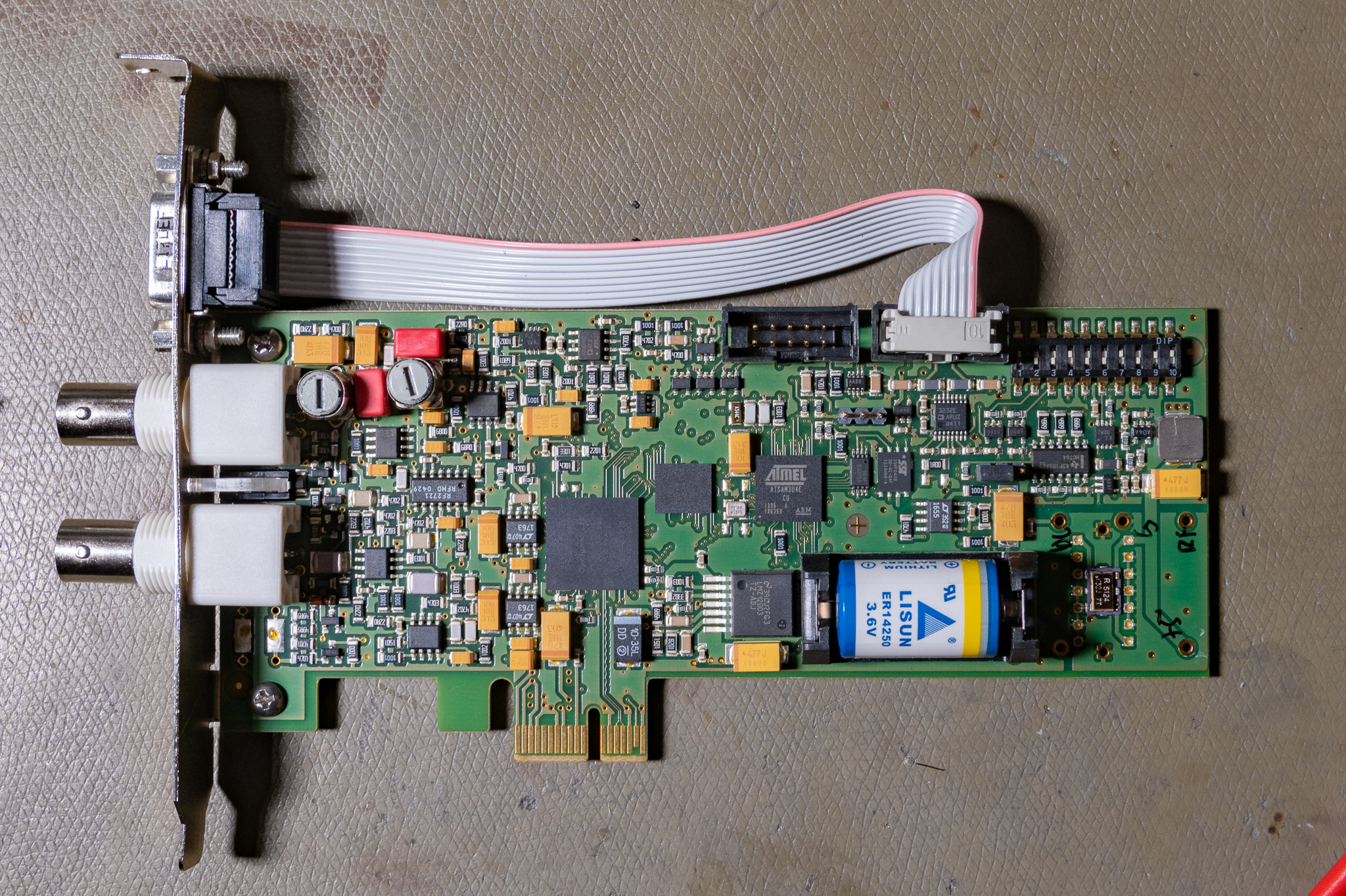
The card is designed to be used with an active antenna provided by Meinberg; in my case this wasn't included, so I use it with an amplified optical detector hooked up to my Mini-Whip (Meinberg uses amplified ferrite rod antennas). The antenna coax outputs 5 V, and it requires a few mA of current draw to not register an antenna fault.
A usable signal level at the antenna port is 10-20 µV (10 Hz bandwidth).
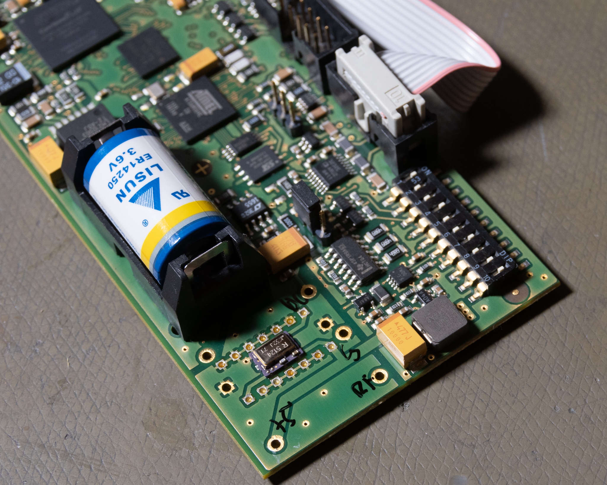
The bottom BNC is a timecode output, which by default outputs IRIG-B format. The D-Sub is fairly flexible and can output standard RS-232 serial timecodes, 1PPS & 1PPM (RS-232 and TTL), 10 MHz (TTL), 5 V supply, DCF & unmodulated IRIG codes, as well as time capture inputs. This is configured using the 10 position DIP switch, and is well documented in the manual.
The base design appears to use an ARM microcontroller (MCU, ATSAM3U4E) along with a Altera Cyclone IV FPGA which has the PCIe interface, and also implements the coherent clock and timecode (DCF, IRIG) generators according to the block diagram. My guess is the correlator is implemented in software in the MCU.
The unused 10 pin connector is most likely a test connector with JTAG for programming and testing the on-board devices, it's simply marked as "RESERVED" in the documentation. It looks like there are a couple of logic gates hooked up to it. The unused 3 pin header is a second RS-232 serial port.
The main RF mixer appears to be a RF2721 integrated phase shifter quadrature down-converter, and there is presumably a two-channel ADC on the board to digitise the I/Q signal (the MCU has a single 8-input 12 bit ADC built in). The remaining analog parts are mostly decent quality opamps, and linear voltage regulators.
The RS-232 interface is as expected generated with a MAX3232.
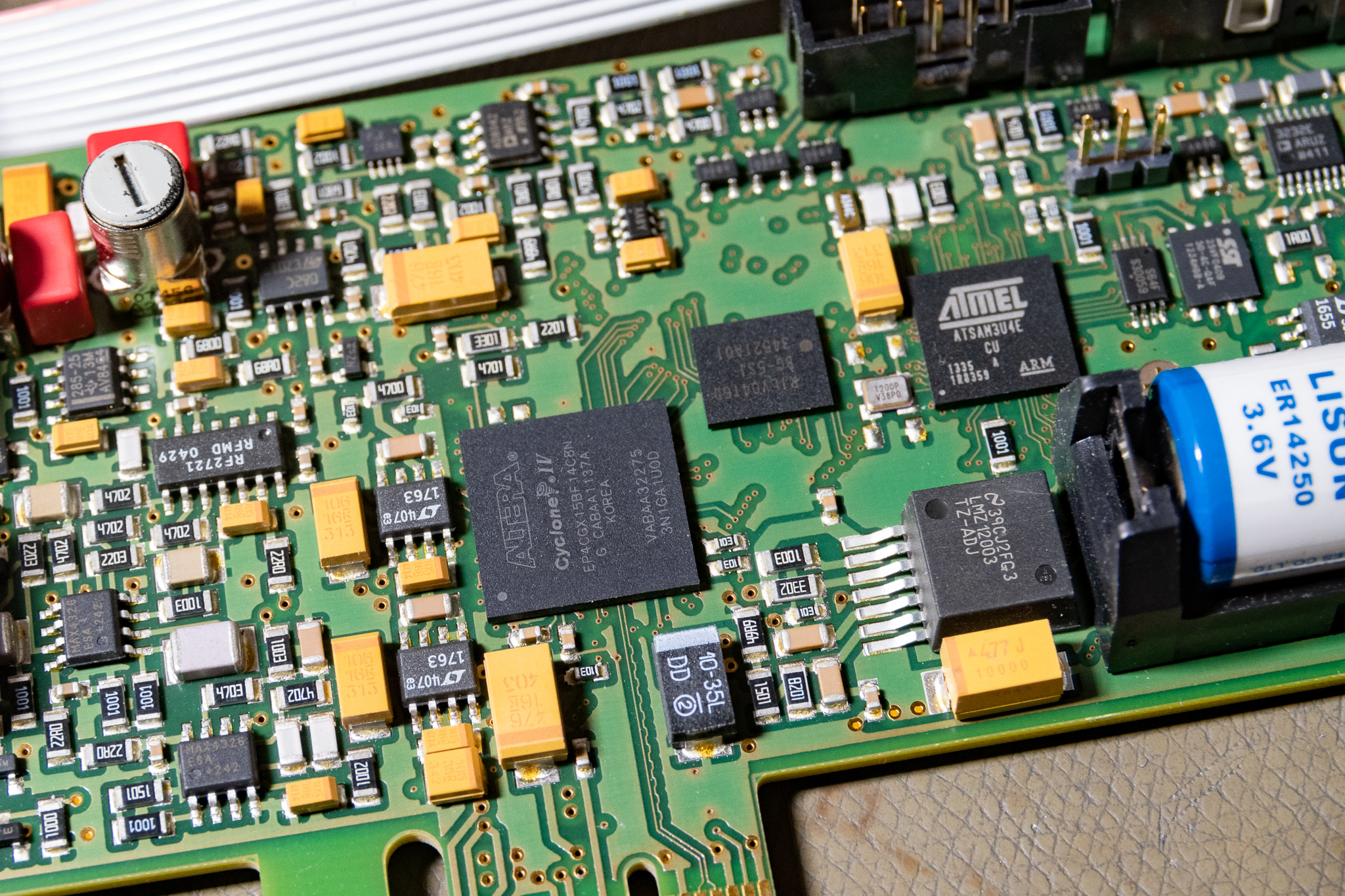
The BGA chip between the FPGA and ARM processor is a R1LV0416D 4 Mbit SRAM, presumably used by the FPGA. This could be a cost reduction measure since while you can get an FPGA with more built in memory than that, it's probably cheaper (but slower) to put in external SRAM.
There is a SST25VF040 4 Mbit SPI flash near the ARM processor, this is likely what stores the FPGA configuration (the ARM processor has 256 kB of internal flash for its own program). The TSSOP-8 packaged device marked "S64F" between the two is a small 64 kbit SPI flash, part no. CAV25640, I assume this is the configuration storage including e.g. serial number and product type.
This split makes sense from a developers perspective, since you can simply overwrite both the MCU built in firmware, and the FPGA configuration flash fully without losing unit specific information.
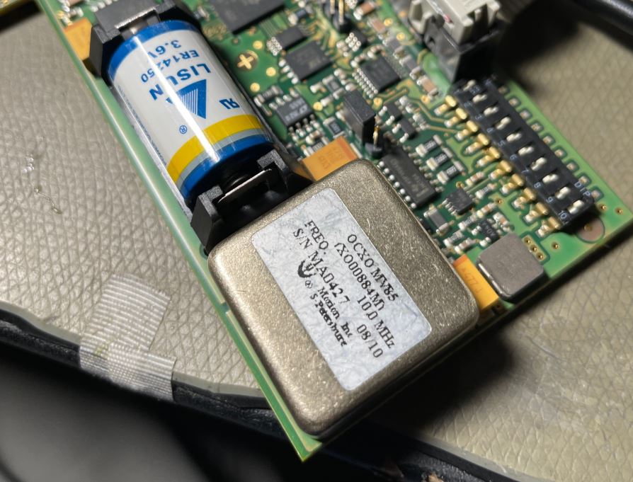
There is a 1⁄2 AA (14250) non-rechargeable Li-Ion battery which presumably keeps the real time clock in the ARM processor running when powered off. This is not required for operation, since my card worked just fine with a dead one. I did replace it since I had a spare sitting around, but it's probably not essential for an always-on setup like mine.
This battery might also power the battery backed SRAM in the MCU to store drift correction info; since they use a standard EEPROM for configuration storage it would not be considered proper to continuously store this information there due to the risk of flash wear-out. The battery also seems to store settings such as the serial port and time code configuration.
OCXO?
This card and I suspect almost all others sold use a VCTCXO timebase, but there are also VCOCXO options you could probably get if you wanted to pay even more.
The standard crystal is a 10 MHz clipped sine output, based on a quick search it appears it might be a CTS model 589 (e.g. 589S100X2CAT). The distinctive package makes it relatively easy to recognise in product pictures, though the markings don't match the 589 series. The actual markings are "R 5124" and "K32J 7T".
A 74HCT04 is presumably used as the amplifier for the crystal oscillator signal.
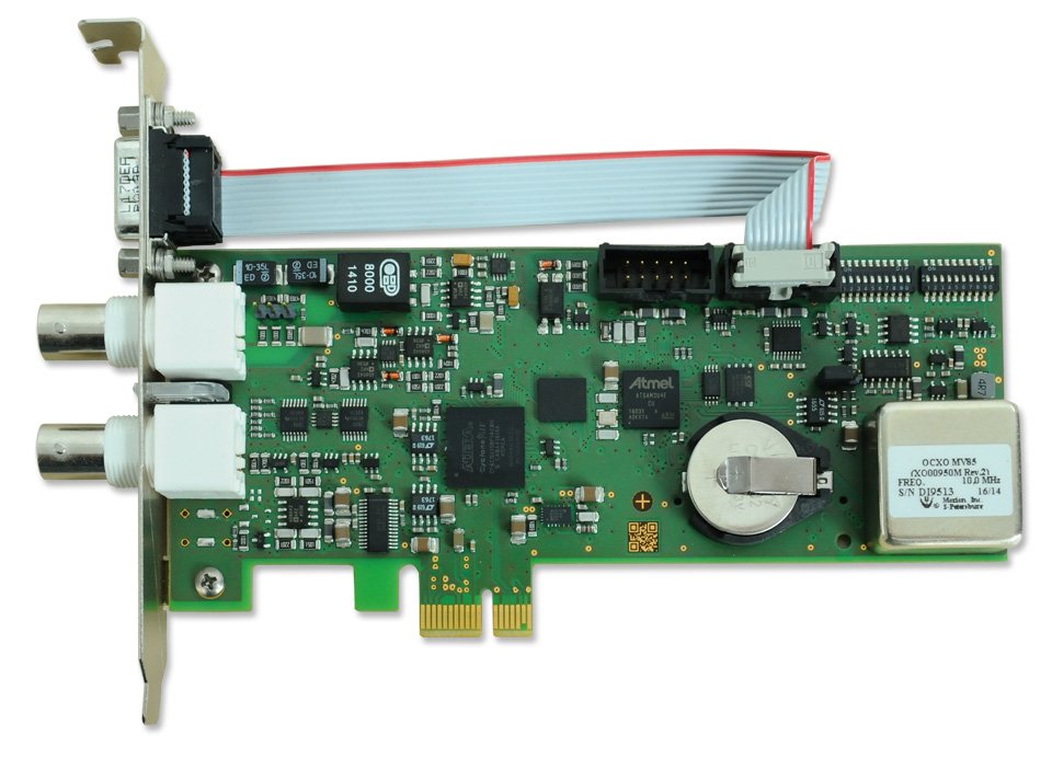
The OCXO pinout appears to match e.g. a Morion MV85, with a 19.05 mm pin spacing and 5 V supply. There is also a 14 pin DIP pinout which could possibly also be used for an OCXO – the documentation mentions 3-4 possible quality grades of OCXO being supported.
Morion's US distributor lists the MV85 as a "Lower cost, high stability miniature OCXO," and the MV331 appears to be the most stable variant they offer in the 25x25x12.7 mm case size at 10 MHz. However, the MV85 is significantly easier to get at an affordable price and has similar specifications to all other variants except for phase noise (where the MV389 appears to dominate).
If you want to buy new, Digi-Key has a few seemingly pin compatible types in stock, such as the Connor Winfield OH100-61005SV-010.0M and the Taitien NA-10M-2503, or perhaps even the Abracon LLC AOCJY3A-10.000MHZ. These aren't cheap but also not ludicrously expensive, sitting comfortably in the $100 price range.
The clearly related TCR180PEX (IRIG-B I/O card) product picture also shows a Morion MV85 10 MHz OCXO installed, which is a pretty good clue (I didn't notice this until I had already ordered a MV85 anyway).
Meinberg has a list of oscillator options for its products, but I'm not sure what the MV85 is classed as; the PZF180 manual says -LQ, -MQ, and -HQ are available meaning they fit one of the two possible layouts. Based on the phase noise and yearly aging specifications it's probably a MQ or HQ quality if we assume Meinberg derates the Morion specifications a bit. The MV85 can obviously be bought in various quality grades.
The LQ quality is likely the DIP-14 option? Fox and Bomar sell DIP-14 packaged OCXOs that have worse specifications than the Morion MV85, approximately in line with the LQ spec.
Based on the specification of the CTS 589, the control voltage range of the VCTCXO is 0-2.5 V, while the MV85 range is 0-4.5 V.
The chip next to the battery is a LTC1655 16-bit DAC, this outputs a voltage between 0 and 4.096 V (internal 2.048 V reference with ⨉2 output amplifier). Assuming the card is willing to use the full range of the DAC for tuning – and isn't soft-limited to e.g. the 0-2.5 V range of the TCXO – it should be close enough. The step size is 62.5 µV, so if you have a system voltmeter you can program a reading in ADC LSBs.
As seen below, the tuning voltage appears to be unlocked, so this upgrade is quite viable.
Most likely the firmware in the ARM processor has some idea of what model the card is and could possibly be modified using e.g. undocumented commands to change its reported type and tuning range, or by dumping the configuration flash.
Stability Testing with stock TCXO
With the TCXO option and reasonably good evening reception, the measured 10 MHz standard deviation was 11 mHz. This was measured with 100 samples at max integration time on a GPS locked HP 5335A. I will note that this measurement is near the HP's noise floor so you shouldn't put too much weight on it. The long integration time of the instrument also means that short term variations are likely to be averaged out to some extent.
Updated: While I did note some random frequency wander etc., with the TCXO, these measurements were later found to be caused by an instrumentation error, and are therefore invalid.
Testing The MV85 OCXO
The MV85 OCXO was quite simple to install, simply hot air reflow off the old TCXO — using kapton tape to insulate the nearby battery holder — and solder in the new OCXO. You likely require hot air, since the TCXO package does not use pins so using solder wick or similar will not work very well and might damage the PCB.
I powered the board up in a CM4 on the bench to let me monitor the tuning voltage. As expected it held the tuning voltage at around 2.5 V until it achieved time sync, and then started ramping the voltage at a rate of ~1 mV every few seconds, slowing down to 0.1-0.2 mV per step (a handful of ADC LSBs) when within around 0.2 Hz of correct.
With a TCXO this sweep rate is likely acceptable, with the OCXO this took quite a while to ramp up to the correct frequency, creeping ever closer over the course of several agonising hours, getting to within +10-20 mHz or so after 10 hours. I'm don't think it was actually "stable" at this point either, rather it seemed like it had overshot the correct frequency slightly and was ramping down again at that point.
Measuring 10 MHz phase drift relative to my GPSDO with a stopwatch and oscilloscope (syncing on the 1 PPS signal), the frequency error was around 1⁄30 to 1⁄60 Hz and going down slowly, which is in the range of 1 ppb. At 10 MHz 10 Hz is 1 ppm, 10 mHz is 1 ppb. Over the next hour it slowed down to a not-measurable frequency error, indicating it can achieve better than 1 ppb frequency error.
I will also note that these frequency error measurement are approaching the expected short term error of my (TCXO equipped) GPSDO, meaning it is difficult to say for certain which clock is actually drifting. My GPSDO NTP server reported a jitter of around 10-20 µs relative to the PZF180PEX NTP server.
Frequency measurements relative to the GPSDO gave a standard deviation of 2-3 mHz over 100 samples (~45 seconds per sample) and around 5-6 mHz over 1000 samples. This is on par with a typical GPSDO receiver measured with the same instrumentation.
Given that this indicates a standard frequency deviation of 0.2-0.5 ppb over several hours, it's possible the (TCXO equipped) GPSDO is performing worse than the radio clock with an OCXO.
I may have to repeat these tests with a Rubidium reference clock to determine which is performing better.
Update: I have since been testing a stable OCXO + a new GNSS receiver relative to the old GPSDO and radio clock. The radio clock seems to drift slightly back and forth relative to these three sources. The magnitude of the drift I have observed is in the 1/30th Hz range or less, which is not an issue for most use cases.
Second update: While testing a new OCXO reference clock I have found that the OCXO equipped PZF180PEX has very good stability. When unlocked, it will accumulate some drift as expected. The slow (10-20 second period) frequency variation I noted above is in fact coming from the TCXO equipped LEA-M8F (and perhaps also the TCXO in the Furuno GT-88). This became quite apparent when comparing phase-error between a C-MAC OCXO, the LEA, and the PZF180: the PZF180 is far more stable.
The 1 PPS phase offset is set in km from the transmitter; it appears the resolution of this adjustment is 5 km, or around 15 µs.
Over all I would say this upgrade is desirable and worth the effort.
One weakness of the clock in my opinion is the lack of any user accessible frequency/time figure of merit information; it only has binary flags for locked/not locked, and does not provide an accuracy estimate.
Raspberry Pi CM4?
The paragraph below is retained for historical accuracy, it was correct at the time of first issue in early 2022.
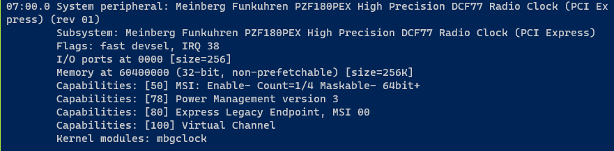
I tried the card in the Raspberry Pi CM4, and it seems like this device requires IO BAR allocations to operate; and I wasn't able to get the driver to load, even using the available flags in the kernel module etc.
It did compile just fine though, Meinberg even has several well written documentation pages on how to compile on various distributions including Raspbian, and the driver seems to be binary-blob free. Presumably this is intended for USB/serial devices which likely work just fine.
It is likely that the similar GPS180PEX/GNS181PEX will have the same exact issue.
The limitation here is in the SoC used in the Pi CM4, which doesn't support PCIe IO BAR registers, so it does not appear to be possible to use this card with this processor at all unless Meinberg develops a driver that can use some other I/O method (technically possible since it has an FPGA interface, but unlikely to happen).
Something like an Orange Pi or another Linux based ARM board with PCIe might work, assuming the SoC in use has IO BAR support. The AllWinner H6 used by some of the PCIe "capable" models apparently has such a weird implementation PCIe that it might as well not be there.
As such unfortunately there aren't too many options for integrating this device with a small embedded computer outside of something Intel/AMD based. An Atom D425 board may be the oldest and cheapest practical solution for this purpose, with a 10 W TDP processor and up to a single 1x PCIe lane available. For the time being keeping the board in my server is not a major issue.
I will note that for some uses cases, you could skip the PCIe part and just hook up the 1PPS, serial port, and 10 MHz frequency output to some other equipment. The card operates mostly standalone if power is applied, but configuration likely requires PCIe.
(2024) Raspberry Pi CM4.
In 2022 this didn't work, I'm not sure what happened between then and July 2024, but it works now! I expect either a kernel update or Meinberg driver update has happened.
Further, the Linux driver seems to have gained a parameter to adjust the transmitter distance recently. This feature was missing previously (only supported in the Windows driver). It's great to see continuing maintenance and development of this software!
Works great, and the CM4 even has hardware timestamping making it a good choice.
SiFive Unmatched RISC-V
Doesn't work here either on the Ubuntu 21.10 distro, some kind of I/O port issue?
Note: not retested in 2024, it's possible newer kernels may work.
Small PC with RHEL 9
In mid-2022 I installed this card in an HP EliteDesk 800 G1, and this worked just fine. I used an eBay sourced PCIe extender to connect it to the mini-PCIe port in this tiny computer.
Using RHEL 9 the driver install from source was unproblematic, and configuration of Chrony was not an issue. The Meinberg driver supports SHM so adding it to Chrony/NTPSec is a single line affair.
The SHM interface requires some SELinux allowances for chrony:
>cat my-chronyd.temodule my-chronyd 1.0;require {type chronyd_t;type unconfined_service_t;class shm { associate read unix_read unix_write write };}#============= chronyd_t ==============#!!!! This avc is allowed in the current policyallow chronyd_t unconfined_service_t:shm { associate unix_read unix_write };allow chronyd_t unconfined_service_t:shm { read write };
You might also want to modify the parameters for the mbgsvcd service.
Edit /etc/systemd/system/mbgsvcd.service to read:
[Service]EnvironmentFile=/etc/default/mbgsvcType=simpleExecStart=/usr/local/sbin/mbgsvcd $MBG_OPTS
Then create the environment file /etc/default/mbgsvc:
MBG_OPTS="-f -q -t 36400"I set it to a somewhat random 36400 seconds, which seemed like a decent number for an OCXO equipped clock.
The service will emit logs when entering holdover, though it will not log exiting holdover for some reason. This can make it hard know how long the holdover state lasted when reviewing logs.
Late 2022 Update: The current development branch of the Meinberg Git has improved the service log outputs, and I believe the bug mentioned below has been resolved as well. At the time of writing, the service parameter file above has not been implemented yet.
I patched the service executable to make it log initial and return of sync separately:
  // Check if the device is now synchronized,
  // and if it is, handle that case.
  if ( check_if_sync( p_status ) )
  {
    // If the device is now synchronized, but
    // wasn't synchronized before, mark the
    // outgoing state as synchronized, and
    // terminate a possible holdover mode.
    if ( !p_ds->synced_after_reset )
    {
      p_ds->synced_after_reset = true;
      p_ds->trust_time_start = 0;
      p_ds->trust_time_end = 0;
    }
    goto setup_ntp_leap_bits;
  }
Was changed to:
// Check if the device is now synchronized,// and if it is, handle that case.if ( check_if_sync( p_status ) ){// If the device is now synchronized, but// wasn't synchronized before, mark the// outgoing state as synchronized, and// terminate a possible holdover mode.if ( !p_ds->synced_after_reset ){p_ds->synced_after_reset = true;p_ds->trust_time_start = 0;p_ds->trust_time_end = 0;mbg_log( LOG_WARNING, "Device #%i: Synchronized after reset.",p_ds->dev_idx);}else if (p_ds->trust_time_start != 0){mbg_log( LOG_WARNING, "Device #%i: Now synchronized following holdover.",p_ds->dev_idx);
p_ds->trust_time_start = 0;
p_ds->trust_time_end = 0;}goto setup_ntp_leap_bits;}
Note that the reset of the trust_time_start/end is optional but I think it fixes a bug in handling the re-entry of holdover following a prior holdover state which was interrupted before trust time expiry.
In this case it seems the service will not reset the trust time interval, but rather use the interval of the first holdover state entry, which could lead to the trust time being 0 if the second holdover entry occurs after the trust time of the first holdover entry would have expired.
This observation and suggestions for an environment file has been reported to Meinberg.
Logging
At the time of writing the current release Meinberg software stack does not appear to time series database compatible logging. To log signal strength, correlation, and lock status I modified the mbgshowsignal program to output a Prometheus Exposition file, which is picked up by Telegraf.
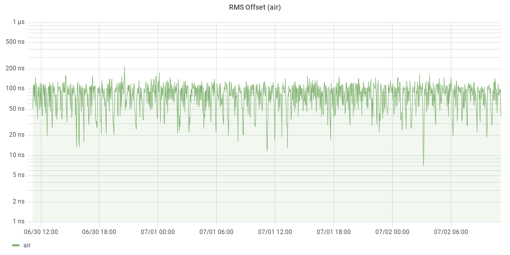
Below is a sample log showing two days worth of signal strengths:
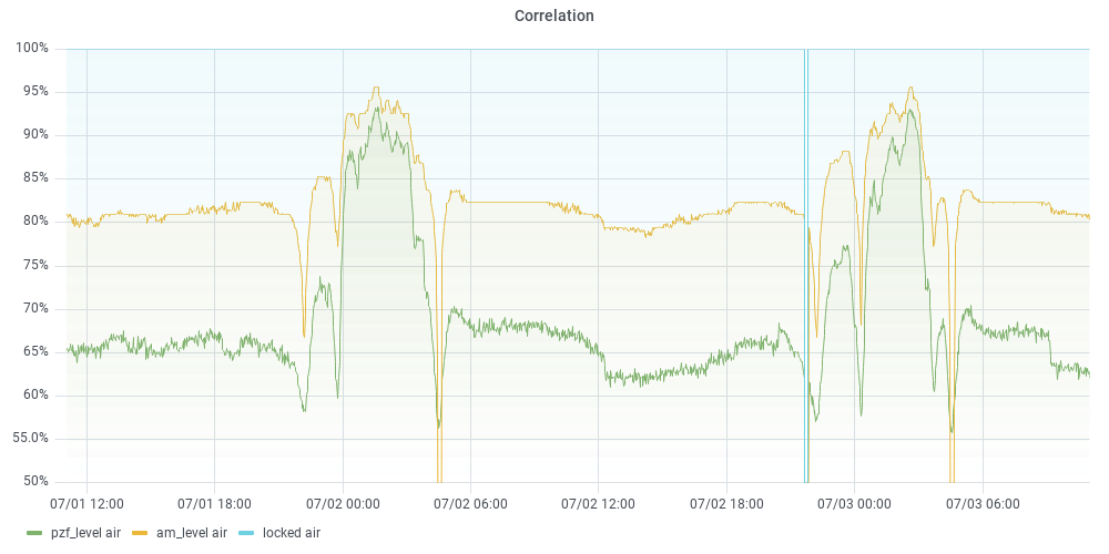
Note that lock was lost at around 21:00 on the last day, this was expected since the antenna systems were powered down for maintenance. There is a distinct multipath signal drop during the evening and morning, this is caused by the changing reflection height of the atmosphere causing the skywave propagated signals phase to change.
At my location the ground wave (relatively fixed) and sky wave (variable delay) signal strengths appear to be similar enough that they can cancel if the sky wave arrived 180° out of phase. The card seems to be able to handle this quite well.
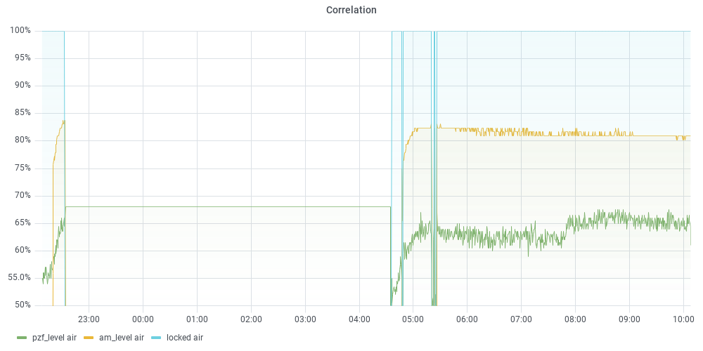
Time stability is better than expected, though I only have chrony RMS time logs to show:
I do expect some variation in offset over time, but it seems the clock is quite stable over time. The measured time offset is close to GNSS clock performance levels.
The higher than expected stability could be explained if the ground wave signal is the dominant component even at my long range.
OCXO Holdover Performance
With the mbgsvcd daemon configured to always output the SHM to chrony, I recorded a several hour long reception outage with the MV85 OCXO mod. This means that chrony was disciplined to the free-running OCXO in the clock for the entire outage, not free-running off the computer clock.
This outage appears to be caused by a seasonal propagation change which likely causes full cancellation of the long wave signal during the night, day-time propagation appears to be unchanged.
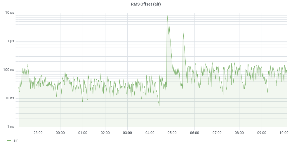
It appears that the clock drifted around 10 µs over a ~6 hour period, or a short term drift of around 1.66 µs per hour, equal to around 40 µs per day.
I will continue recording data and may attempt to generate some plots of daytime vs. nighttime signal strengths over e.g. a year once I have the required data.
Interfacing
Unfortunately for the time being the card has to live in my server, since it can't just be hooked up to a CM4 and live in a little rack cabinet.
I had planned from day 1 to use this card as a time source for my fiber optic clocks, and the interface needed to generate this signal is obviously all custom. Standards like IRIG are for suckers.
As such I made a little adapter to handle:
- 10 MHz capture
- 1PPS capture
- Meinberg Standard Time Code (well documented, easy to parse) to proprietary format conversion (barely documented, non standard, subject to change)
- Modulated onto a single mode fiber or coax
- 3xLED outputs for status
It also includes some spare features to allow future expansion, such as:
- 3xCoax line drivers for frequency or 1PPS output (or DCF/IRIG)
- 3xCoax line driver/receivers for use in e.g. the existing LEA-M8F receiver
- SPI LCD interface (FFC cable)
- Spare RS-232 serial pin header
- I2C pin header
Because of these additional features I decided to built 3 of these, figuring they would come in handy later as well. They could for example be used to interface Epsilon clocks or similar devices.
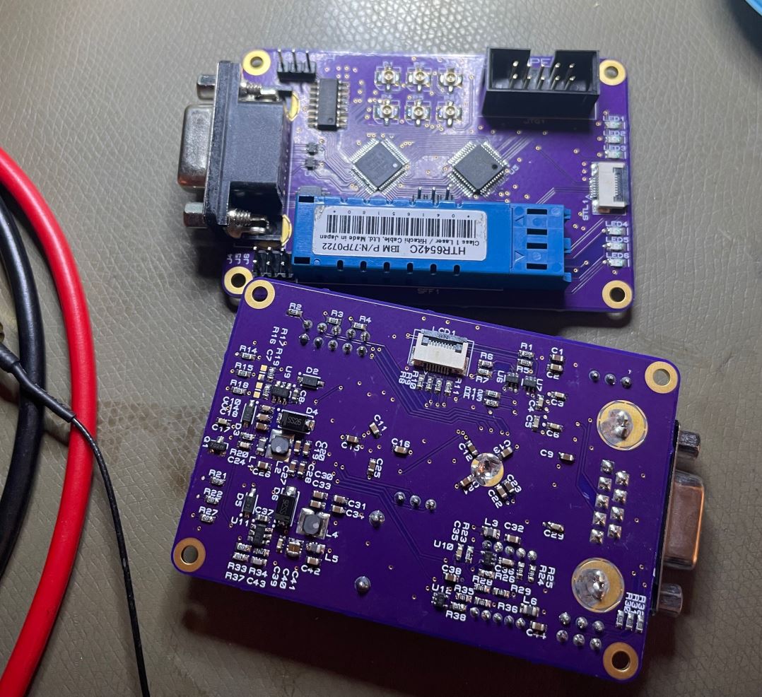
The card runs off the 5 V supplied in the D-Sub, and fits into a Hammond extruded aluminium box. I use a custom made D-Sub cable with coaxes per signal to hopefully improve the signal integrity a bit.
Meinbergs documentation was more than adequate, and I also took the chance when testing the CM4 interfacing to poke around with the scope to verify that things were in fact as documented, and to work out the OCXO pinout.
The board uses a STM32F103C8T6 for the serial port handling (and future expansion), and a MAX V CPLD handles basically all I/O. This makes routing very comfortable, since the CPLD has basically no special purpose pins outside of clock inputs and power (and ground is in the center pad). As such we can pin swap as much as we want, and I generally hook up as many pins as possible between the CPLD and MCU, using the CPLD as an I/O mux for maximum flexibility later.
I use the MCUs built in PLL to increase the 10 MHz input from the PZF to 40 MHz for the CPU core clock, and this is fed back to the CPLD and used as the time base for the 10 MHz output. The CPU could do higher, but this allows easy division in the CPLD.
This is done since I generally want to have a higher clock frequency available for the logic, and also since the duty cycle of the 10 MHz output was not exactly 50% (closer to 40% with the TCXO). This could cause issues with the fiber optic interface, since it's AC coupled and can't pass a 40% duty cycle properly.
By multiplying up to 40 MHz and dividing by 4, an exact 50% duty cycle is guaranteed. The downside is that we potentially add some phase noise to the signal, but this 10 MHz output is only used as a PLL reference, so any noise added will be rejected there.
Keeping the MCUs core clock synchronized with the CPLD logic also ensures that the UART data output is exactly on frequency and coherent to the 10/1 MHz FSK frequencies.
The MCU will have a problem if it's powered on for a while with no external clock available – in order to alleviate this problem the built in clock security system could be used. These MCUs always boot on their internal RC oscillator, and typically switch to external clocking with PLL etc. as part of the startup code. The CPLD could also be used to implement a MCU reset routine (the CPLD can assert MCU RESET in this design).
My fix for this problem was to simply enable the independent watchdog peripheral before doing any clock switching — if the external clock is not present or not usable, the MCU will simply reset after a second or so. Eventually, the clock will be good enough and it will start up properly.
Over all the software to achieve my goals of seeing a NumiClock show the time took 3-4 hours to put together.