The 3021N RF Section/1st Converter (Part 7)
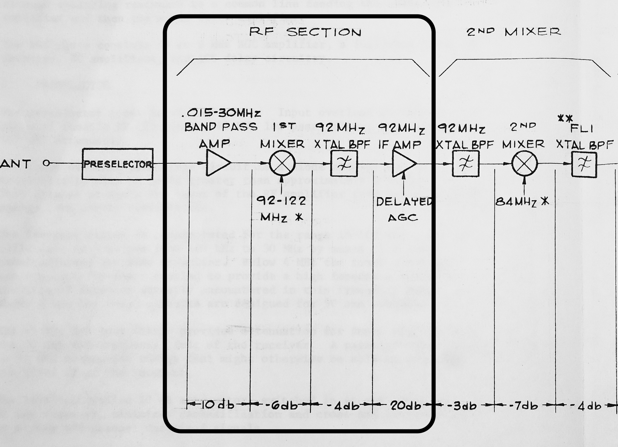
The RF Section or 1st Converter consists of the pre-amplifier, first mixer, and first IF filter in the receiver signal chain. This is typically the most important part of the radio since it determines the sensitivity and selectivity of the radio.
This card was finished in late 2022, at the time of initial publication it has not been integrated yet.
Table of Contents
The Original Design
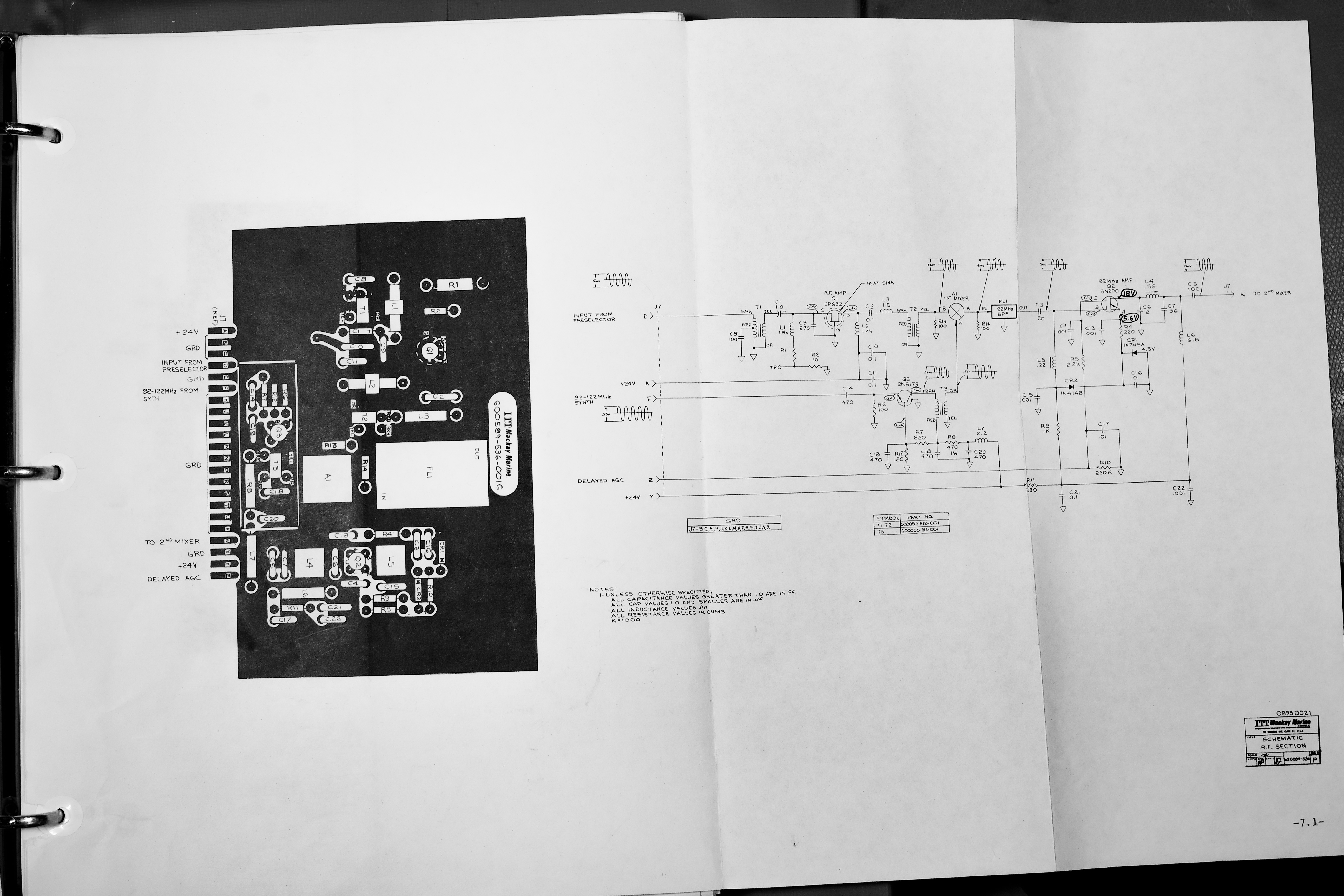
The original 1st converter (RF Section) was built using a JFET pre-amplifier, and a double balanced diode-ring mixer. A crystal filter and dual-gate MOSFET post-amplifier were used for AGC.
Transformer impedance-matching was used for the preamp, for much the same reason as I did in the new design.
The filter bandwidth of the original design was around 6-8 kHz, slightly wider than the 2nd Mixer crystal filter.
The New Design
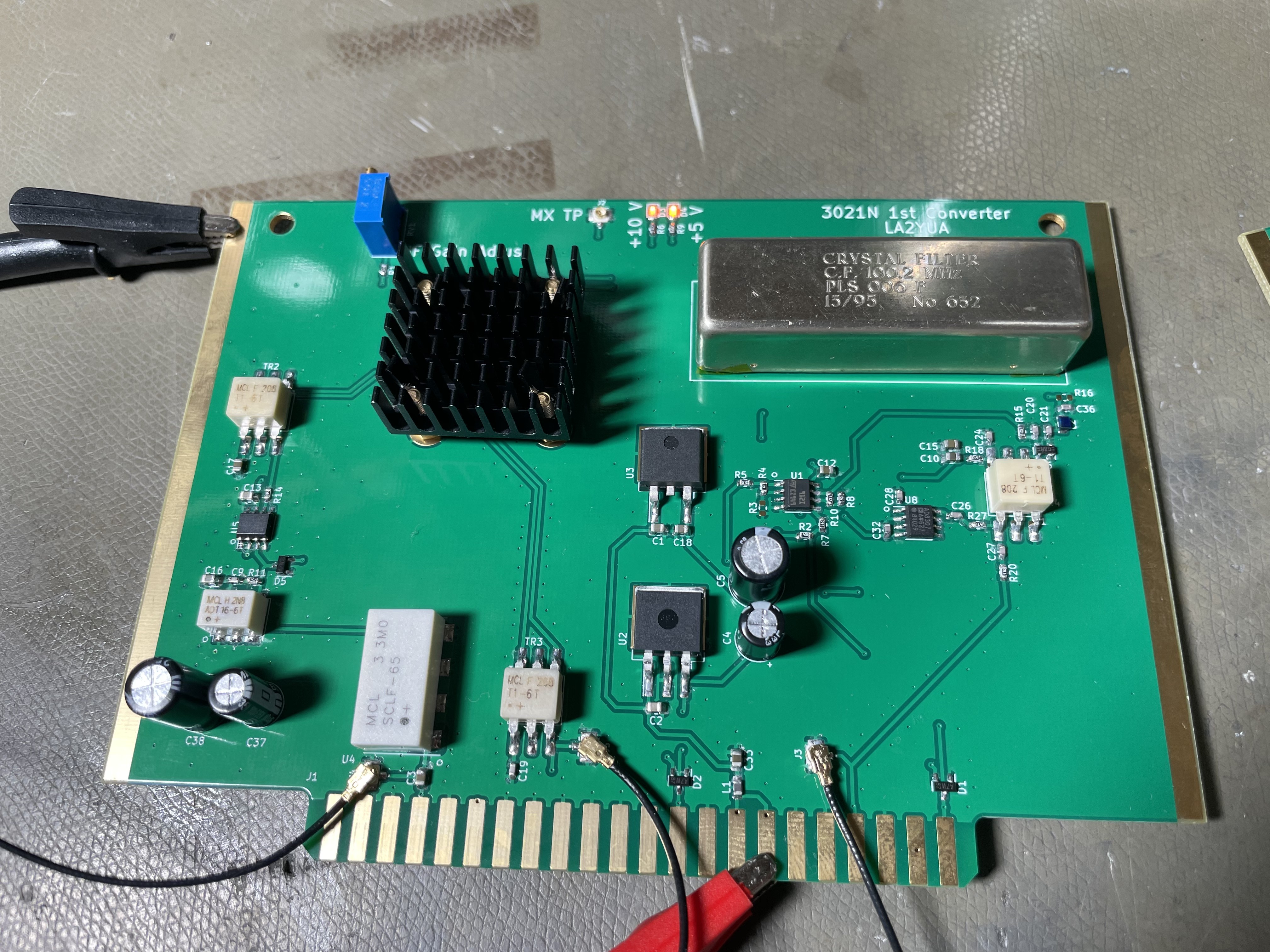
The new 1st Converter was designed as part of the solution to the problem of the rather poor IF filter performance that has been mentioned previously in the Synthesizer article. When I acquired the new crystal filters I figured this would be a suitable place to test them, and I was also interested in a higher sensitivity input stage.

The new 1st Converter is more or less a 1:1 replacement of the old one, with the primary functional difference being a new 1st IF frequency of 100.2 instead of 92 MHz, wider IF bandwidth, and a RF frequency range of up to 60 MHz. This card also uses a 12-15 V supply voltage instead of the previous designs 24 V supply.
Pre-Amplifier
The converter features a high sensitivity pre-amplifier built using an OPA847 that is driven through a 1:16 impedance transformer and giving a gain of around 30 dB.
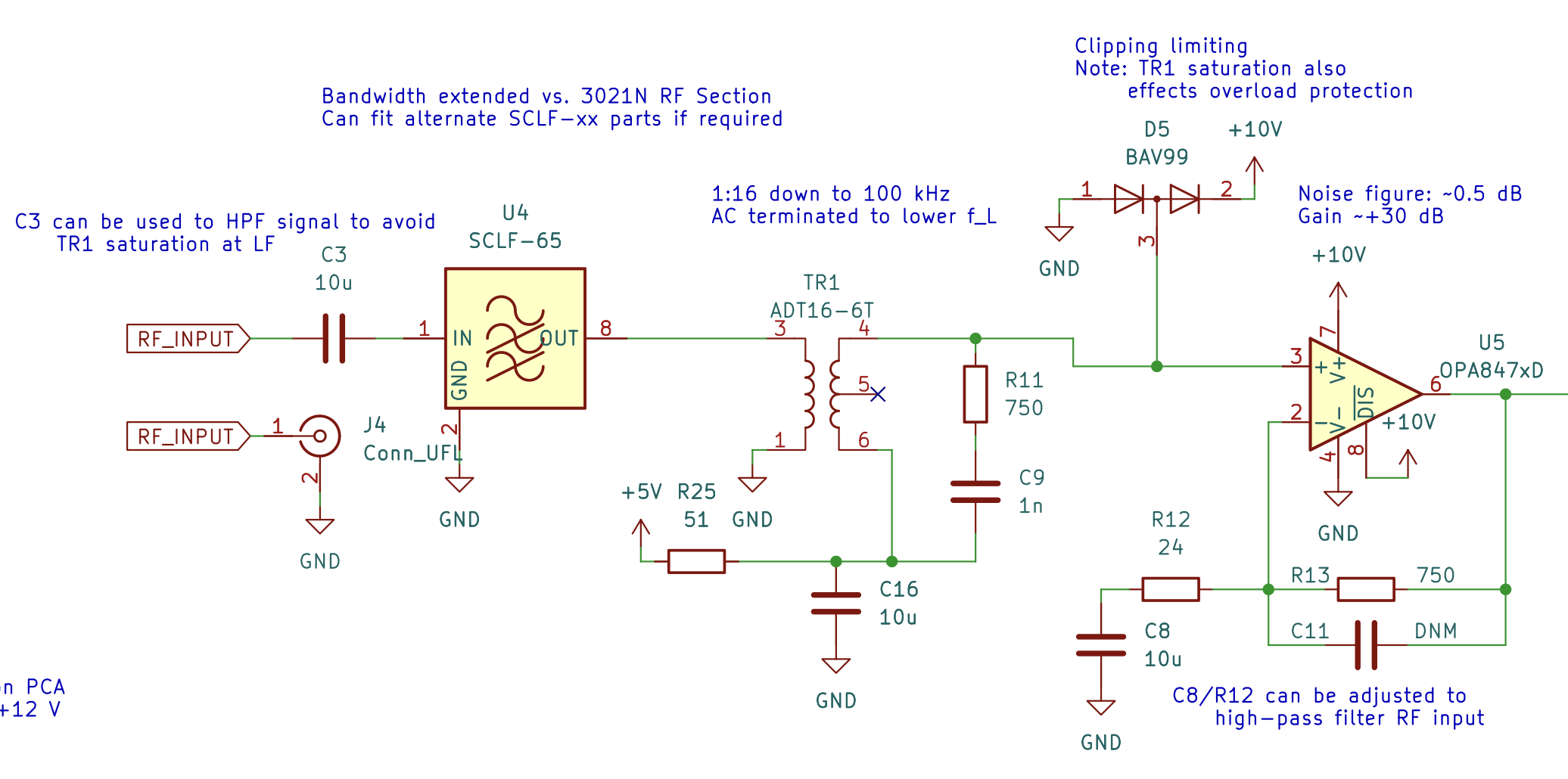
The frequency coverage is approximately 15 kHz to 60 MHz, slightly extended. The RF transformer is the Mini-Circuits ADT16-6T, which is AC-terminated to 800 Ω on the secondary, this AC termination extends the low frequency pass band a fair bit at the cost of strong signal handling capabilities.
A SCLF-65+ low pass filter is used on the input to limit VHF interference.
The use of the transformer increases the source voltage level, and this reduces the effect of the operational amplifiers input referred noise voltage. The benefit of this amplifier is the high linearity, due to it's closed loop operation.
Mixer
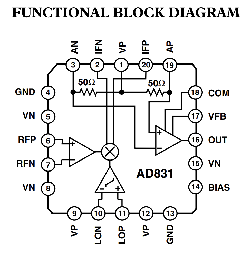
The amplified RF is applied to the AD831 high linearity mixer, which multiplies the RF with the LO1 signal from the synthesizer.
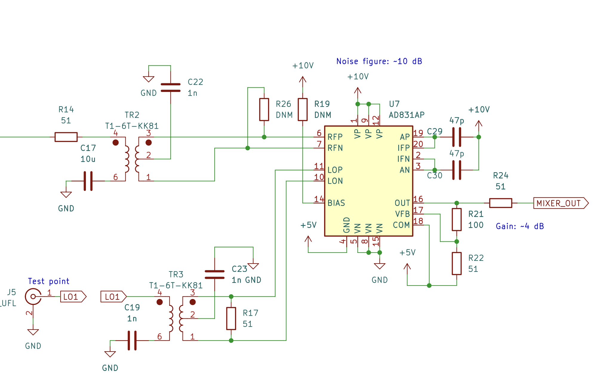
For æsthetic purposes I used 1:1 RF transformers for the RF and LO signals. The mixer is operated in the highest linearity mode, which makes it dissipate around 1 W of power, so a large heat sink was designed in. This is larger than required but it was already available and there's plenty of room here.
IF Filtering
The IF output is routed through a Romanian (assumed) made "PLS 006 F" crystal filter with center frequency of 100.2 MHz, I acquired a few of these filters from eBay. These are installed in soldered turned pin sockets and retained with the M2.5 studs applied. A conductive foam gasket is used to as a spacer and to ensure a solid ground connection for the filter case.
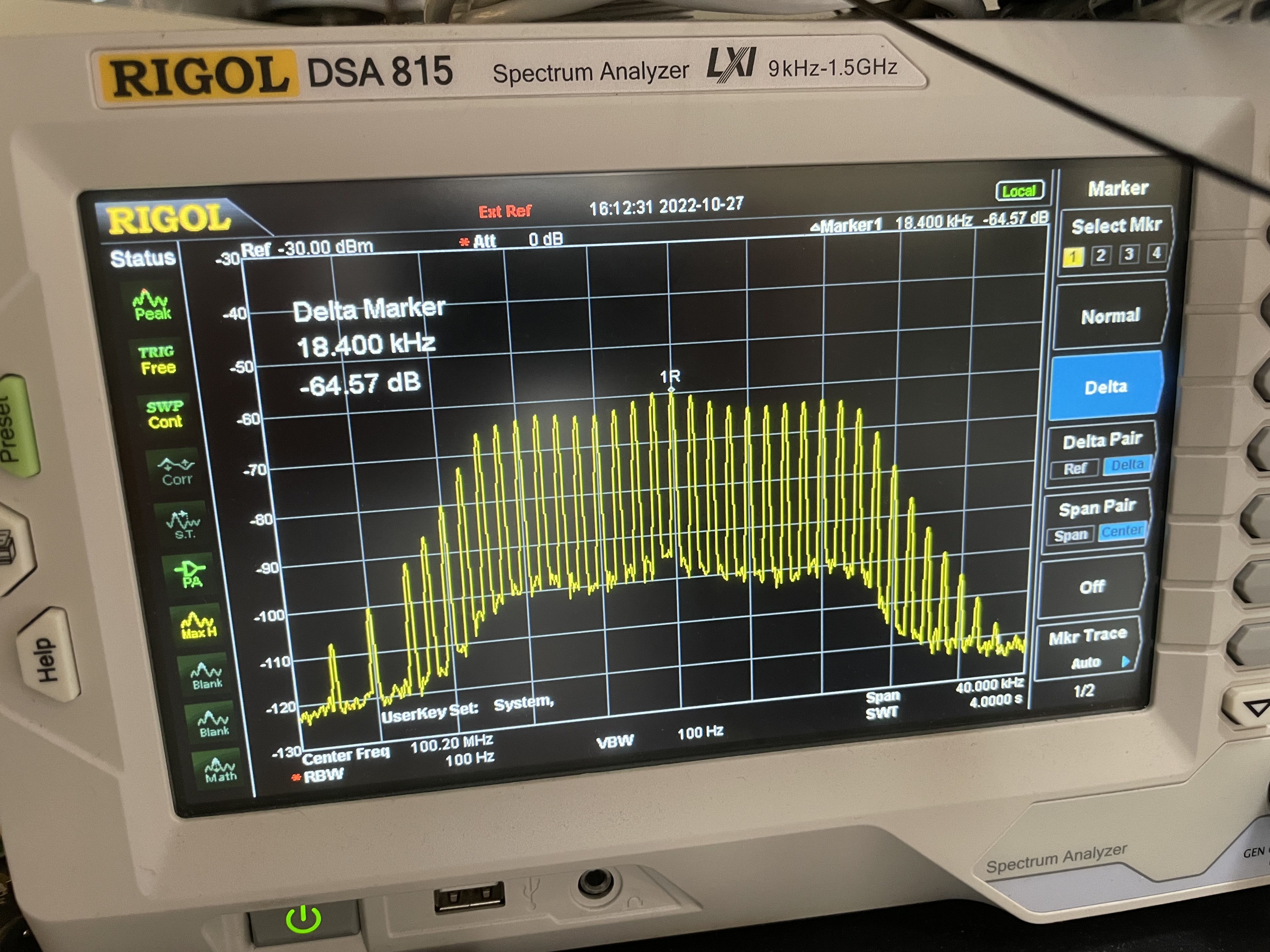
Seen above is a manually stepped frequency response plot of the IF filter, it has a flat 6 dB bandwidth of around 20 kHz (±10 kHz), with high out of band rejection.
IF Amplifier
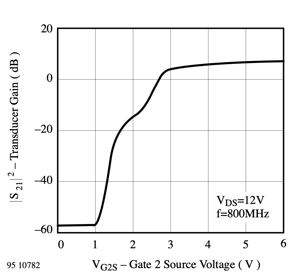
The filter output is amplified further in the 1st IF amplifier, which is a dual gate FET MMIC of type S982 made by Temic. The effective maximum gain is around 20 dB, while the total gain control range is around 60 dB.
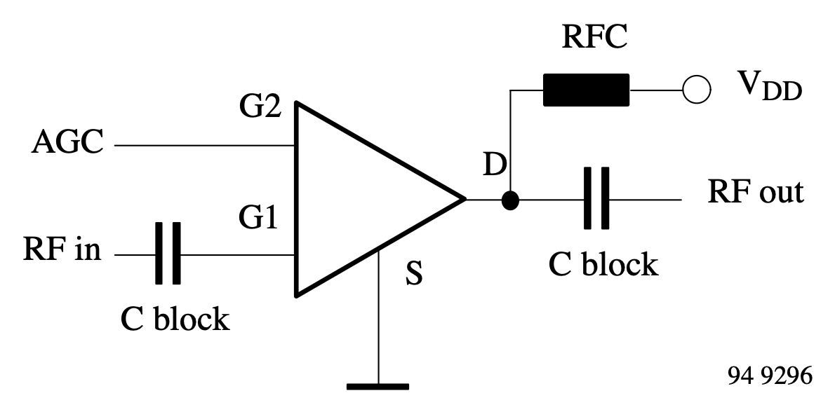
This is a self-biased dual gate FET amplifier suitable for use up to around 1 GHz, and a basic L-match is used to match the 50 Ω filter signal to gate 1 to increase conversion gain.
Gate 2 is the AGC signal, and is controlled by the 2nd IF Processor, though a potentiometer on the board will drive it if no external signal overrides it. This simplifies testing.
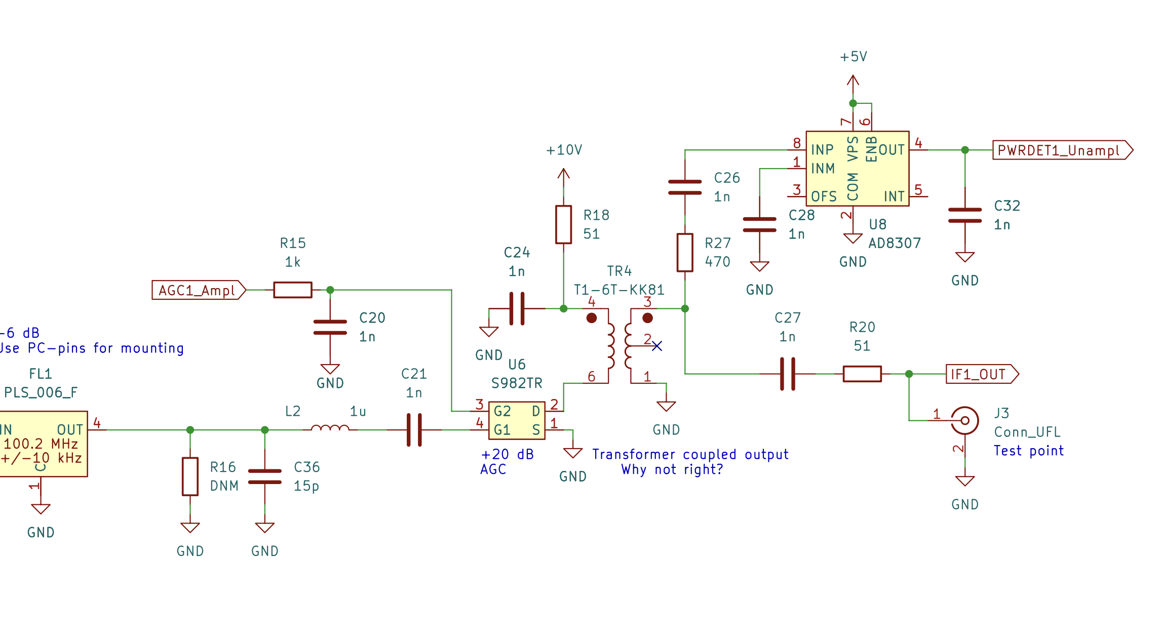
In this design I used a 1:1 transformer as the RF-choke for the device, and the signal is output on the secondary side. An AD8307 RMS detector is also connected to sample the RF power here, which can be used by the 2nd IF Processor to quickly detect saturation.
External Interface
The external interface for operational use is a card-edge connector with 0.157" pitch, fairly standard for the era. Power is supplied at 12-15 V DC, and there is an RF in, LO in, and IF out port.
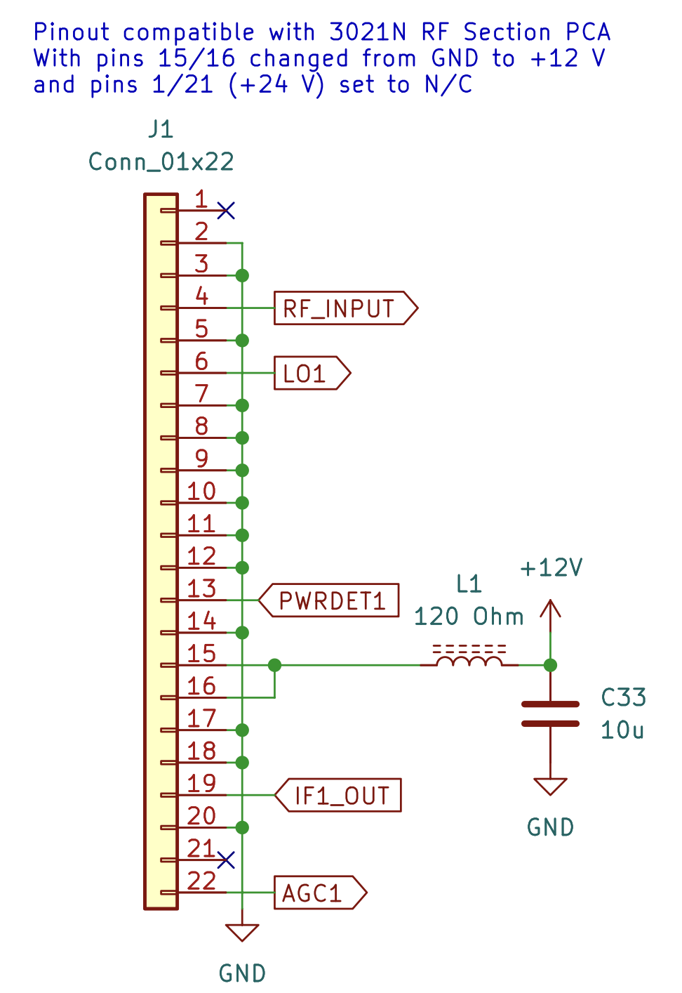
In addition, there is an AGC control input (from the 2nd Converter) and a power-detect output which can be used by the 2nd Converter but probably won't (it doesn't measure anything the converter can't work out on its own).
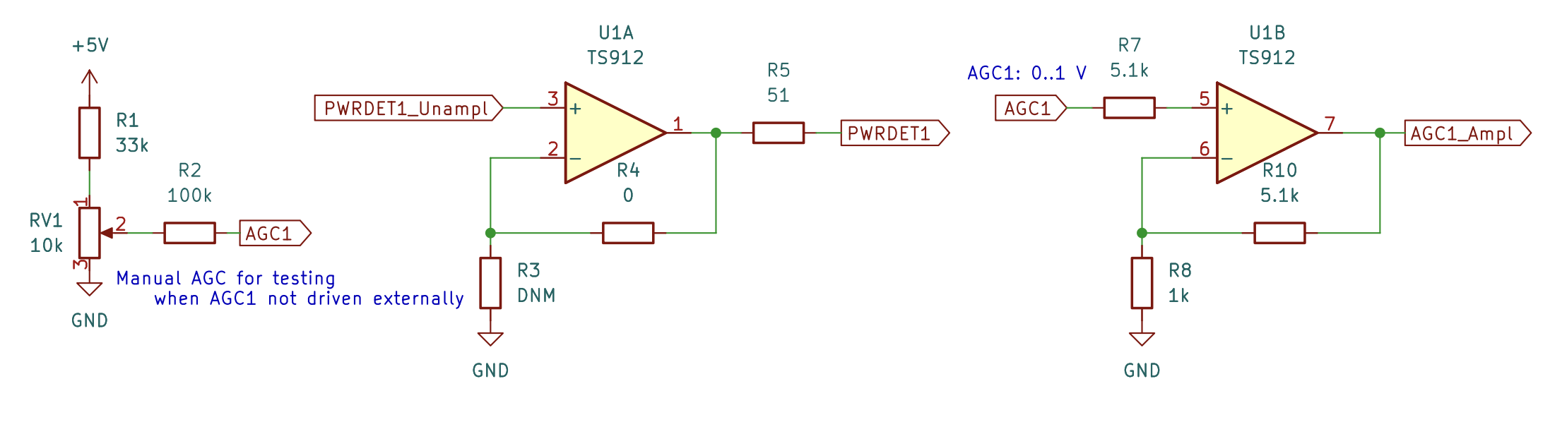
Above the analog interfaces are shown, the PWRDET1 (for IF 1) is a buffered AD8307 signal, and the AGC1 external input is 0-1 V, with the amplifier applying adequate gain matching the S982 MOSMICs control range.
AGC1 has a weak link to a potentiometer, so when undriven for testing this potentiometer can be used to manually set the gain.
Performance
Performance testing indicated that noise floor is very low, as expected, and conversion gain is sufficient that it can easily be digitised in the next converter.
However, the design may be slightly front-loaded wrt. gain so I may go back later and reduce the pre-amplifier gain to improve interference handling.