Using the WM8804 S/PDIF Transceiver in Full-Duplex Mode

The WM8804 is a now obsolete but still available S/PDIF transceiver that is kind of mid but can be made to work ok for some use cases.
My biggest issue with this device is the poorly written datasheet, which makes understanding how the device is meant to work harder than needed. Information is spread all over the place, and some register names are plain wrong (CLKOUTDIS = 1 means enabling the clock output).
It's a shame that the device can't generate the S/PDIF status bits, since otherwise it could have been a nice way to multiplex a low speed UART onto a single pair.
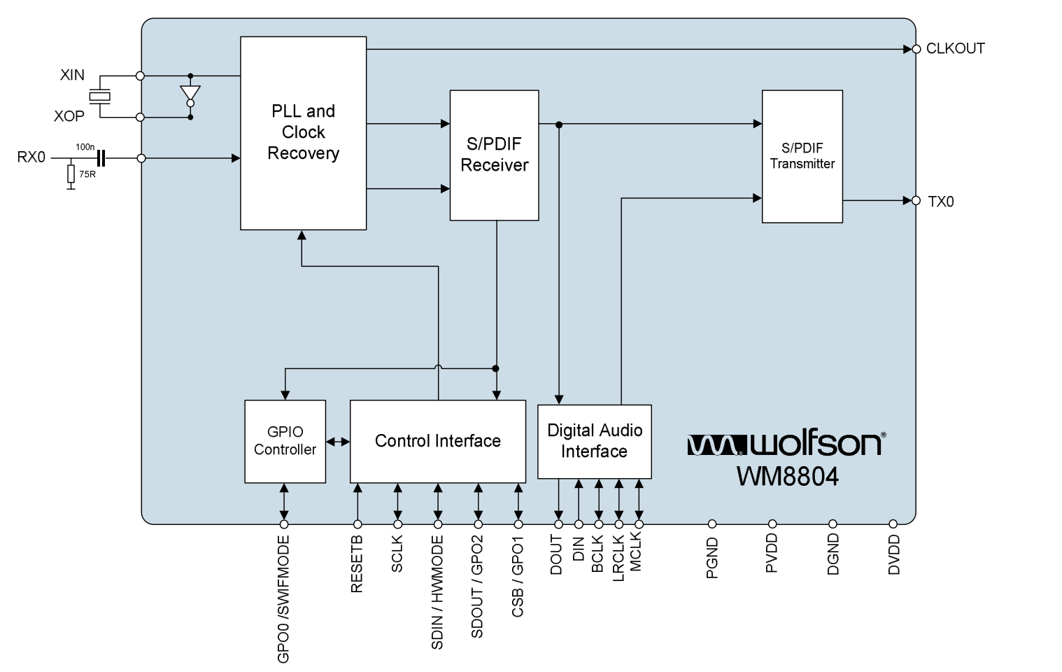
A single WM8804 is capable of being an S/PDIF receiver or transmitter. If you want to use it as a full duplex transceiver, there are severe restrictions.
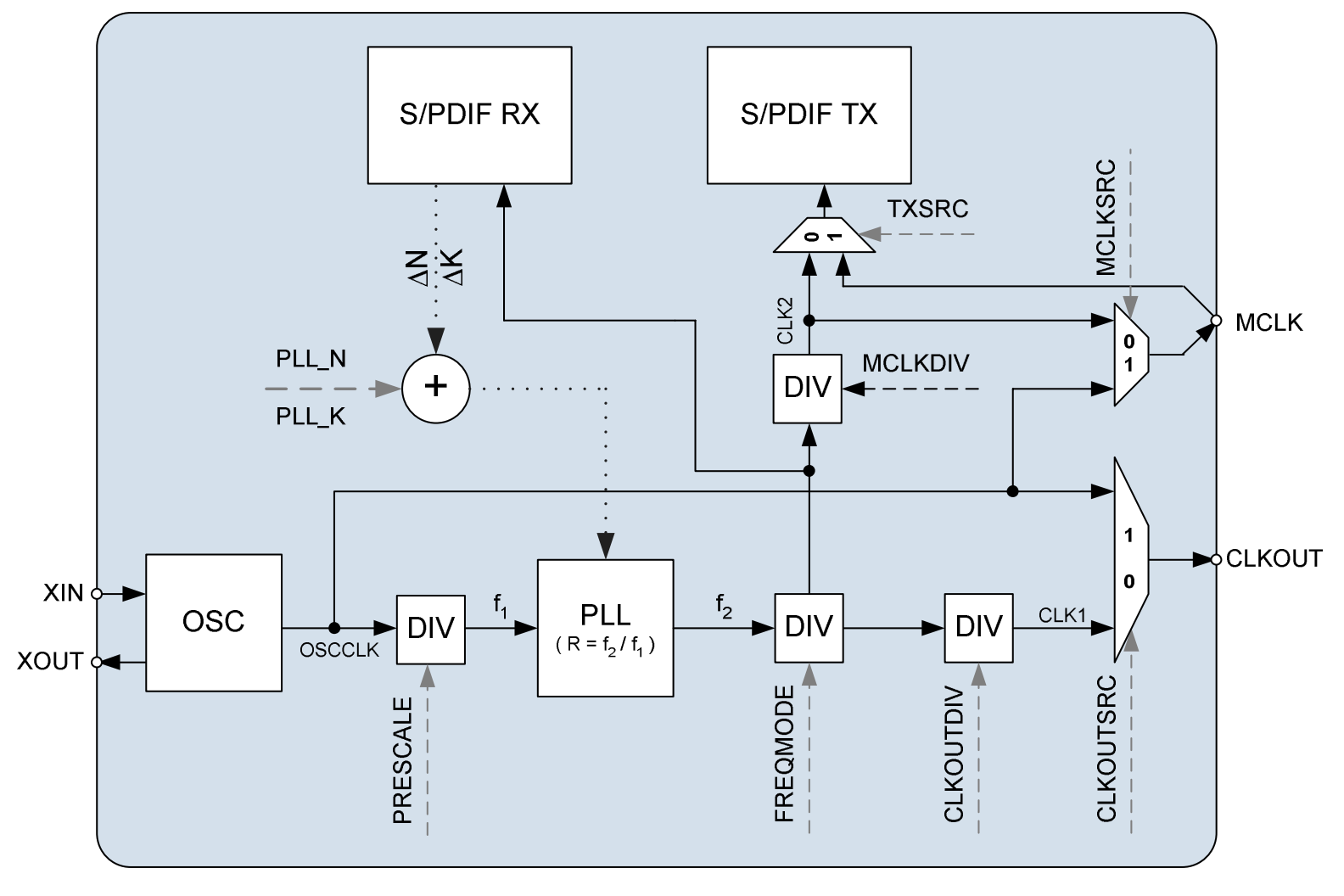
This device uses a fully digital PLL system to lock onto the incoming signal, where it seems to adjust the fractional-N components digitally to generate the required receiver frequency. What this means is that the receiver PLL adjusts the same registers that are available on the external interface.
The receiver is not able to lock without a bitstream. This is fine, the problem is that starting the receiver and PLL without a bitstream makes it randomly output 24 or 48 MHz instead of 12.288 MHz. Once locked it will be fine, and it can coast just fine without a signal after that (assuming no noise, which the datasheet warns about).
To start the receiver without a signal, consider adding a digital loopback from the transmitter pin to the receiver (there's no internal one, despite the obvious issues).
The datasheet makes a big deal about using a common 12 MHz crystal. This is fine, but for a full duplex use case it only has a single fractional PLL. This means that if you try to connect two of them together, they will be trying to lock each other and will quickly wander off. It's not possible from what I can tell to make one device not use the PLL for receive. I'm not sure why the 12 MHz crystal is a big deal since there's no price difference, unless they intended it to be paired with something else that did need exactly 12 MHz.
There's a lot of pitfalls in starting up the IC, incorrect sequencing seems to lock up some of the digital circuitry requiring a hardware reset.

Making one side be the link "master" we can use a configuration that works assuming you control both ends:
The master side configuration will then be:
- S/PDIF in I2S Slave mode (AIF_MS = 0)
- You need a DSP/Codec that can generate the I2S BCLK and LRCLK for the rate you want.
- Crystal: 12.288 MHz (256⨉48 kHz) (can be externally clocked as well)
- If you use 12 MHz, you will get ~47 kHz
- Connect CLKOUT to MCLK direct from crystal, CLKOUT sourced from OSCCLK
- PRESCALE=0, CLKOUTDIS=1 [sic], CLKOUTSRC=1, FREQMODE=2, FRACEN=1
- I.e.: no PLL used for the transmit side, only for receive
- You'll probably want to configure the RX PLL based on datasheet information in any case, but it only needs to be approximately right since it'll lock in anyway.
- Keep the transmitter enabled, do not enable the receiver until the far end has a RX lock
This makes the OSCCLK output and MCLK used by the transmitter 12.288 MHz, the internal PLL is then not routed outside the WM8804.
The slave side configuration will be:
- S/PDIF in I2S Master mode
- OSCCLK 12.288 MHz, but can be 12 MHz since we will use the PLL
- I don't think you need to configure the PLL very accurately, the defaults may be close enough but I did set it up in my software before enabling it.
- Use MCLK to clock your ADC/DAC/DSP
- Clock transmitter off recovered PLL clock
- Keep restarting the S/PDIF receiver until a lock is achieved.
This configuration works but can't start on its own. The way this clocking works is that the master side starts up and generates a valid S/PDIF transmit signal. Once the slave end has locked onto this signal (and we know this through out of band signalling) and is transmitting a signal, we can lock onto that in the master.
This configuration then uses the master clock as a reference, the master transmitter is then coherent to that oscillator. The receiver will be incoherent initially, when locked this receiver's PLL will be running coherent to the master transmitter, and the output from the slave will be coherent to the master receiver. This means there is no real need for a receiver PLL in the master.
The master side needs to have a clock source or crystal that can generate the desired rates without using the internal PLL, which is why a 12.288 MHz crystal is recommended. This also works if you have a 12 MHz crystal, but the sample rate will then be ~47 instead of 48 kHz.