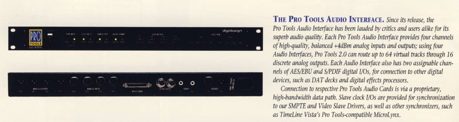
Digidesign/Pro Logic Quad Audio Interface (Four-By-Four (442 Audio Interface (MH031 (4⨉4))))

In this article I'll take a look at the Digidesign Quad Audio Interface, also known as the Four-By-Four.
Overview
The Digidesign Quad Audio Interface, known internally as the Four-By-Four, and later sold as as the Pro Tools Audio Interface after a rebrand/acquisition, is a 4 by 4 audio interface. It is sometimes called the 442 Audio Interface, and may be found listed as a MH031 interface. It may also be sold under the Pro Logic brand, and is often called the 4x4. It is also on occasion referred to as the 442 I/O.
The following is an excerpt from the now defunct Digidesign database:
Specifications for 442 Audio Interface.
The 442 I/O (MH031, 4x4) is the audio interface used in the original Pro Tools system (sometimes called Pro Tools II). It can also be used with an Audio Card (SA4) in a PTIII system to provide 4 additional inputs/outputs. (Requires a TDM single piggyback. Doesn't add DSP or voices.)
Analog Input/Output: Active Balanced XLR (pin 2 hot); +4dB level.
Analog I/O Impedance: Differential 200kohms, single ended 100kohms (input); 22ohms per leg (output).
Digital I/O: 16-bit, Active transformerless inputs (AES balanced, S/PDIF unbalanced), transformer coupled outputs (both).
AES pinout: Pin 1 gnd, pins 2 & 3 balanced signal (not polarized); impedance 110ohms.
External Sync: 256x sample rate (Super Clock) in/out, about 3 Vpp, BNC connectors.
NuBus Card Connector: 50-pin, SCSI2-type female.
Sample Rates: 44.1k or 48k.
Analog-to-Digital Converters: 1 Bit, Delta-Sigma, 64x Oversampling, 16-bit output.
Digital-to-Analog Converters: 18-bit, 8x Oversampling.
Operating Level: +4 dBu nominal (factory calibrated at 14dB or 18dB headroom).
Maximum Levels: +26dBu (input), +24 dbu (output).
Frequency Response: 20Hz - 20kHz +/-1db.
Signal-to-Noise Ratio: > 93 dB A/D, > 108 dB D/A (A Weighted).
THD + N: .005% A/D, .003% D/A.
Power requirements: 100, 120, 220, 240 VAC, 10-60Hz, 16 watts, auto-switching. The power supply is a Skynet model SNP 3034
Dimensions: 1U external rack mount device; 19" x 8.5" x 1.75".
ID:54 Created:12/03/1993
The unit was introduced around 1990, and as mentioned in the specifications, it provides 4/4 analog I/O, it features external clocking options, and AES/SPDIF I/O. The digital I/O is routed through channel 1/2 when active it seems.
This is a fairly pure audio interface, and it uses a proprietary interface over a SCSI2 50 pin connector. The other end of that cable by all accounts has to go to a "442 Audio Card", a special DSP card manufactured for Mac II and Quadra computers with a NuBus expansion interface.
Without this card the interface is largely useless, though as we'll see the I/O is fairly simple so it would probably be possible to interconnect this box with a suitable I2S interface.
Someone looked into this on the diyaudio forum: digidesign 442 I/O as standalone DAC for S/PDIF transport, the thread was first posted in 2004, but the last update was in 2020 where it seems they were successful in hooking up a Raspberry Pi to it.
Table of Contents
Externals
The 442 is a standard 19" 1U rack mount device, the power supply input is standard universal voltage. The finish is "nice black" according to the PT2 flyer.

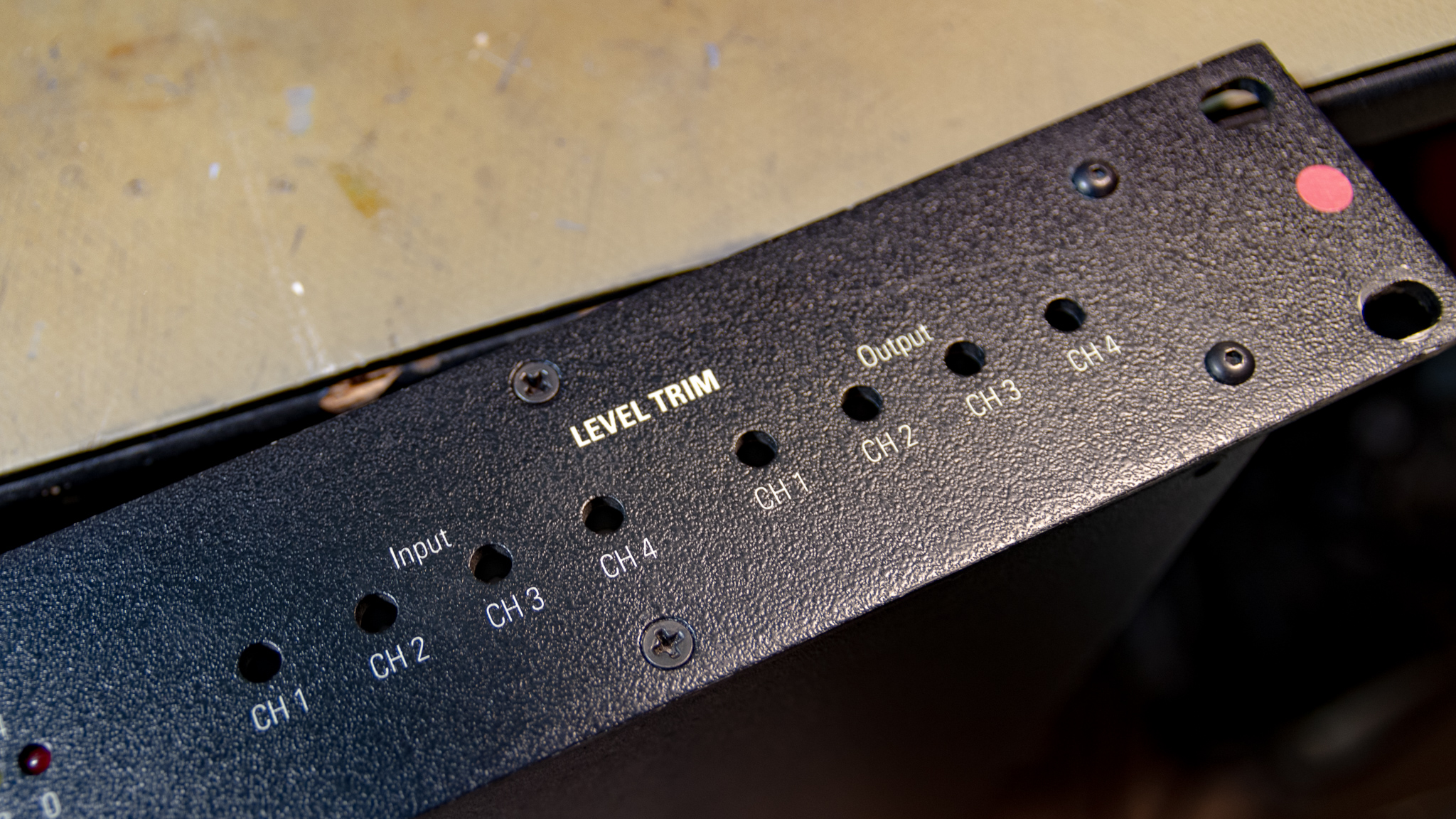
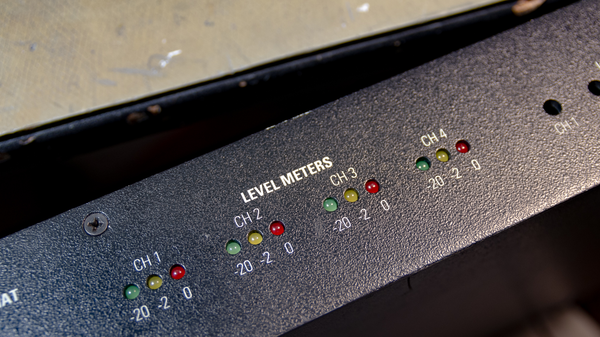


The front panel has a single power button and several LEDs which indicate things like sample rates, digital I/O mode and routing, and levels. There are 8 trimpots accessible through the front panel to adjust the levels of the inputs/outputs. This appears to be intended for fine tuning, as the range is not huge.
The inputs are line level, so I think a dedicated preamp would be preferable for direct microphone recording.
Looking at the design, I doubt the inputs would work with 48 V phantom power applied, though I don't think any damage would occur it would probably give very poor audio.
Note that the word clock I/O is listed as 256⨉fS, this is unusual but was probably done to avoid needing an internal PLL to accept external clocking. 256⨉fS (12.288 MHz @ 48 kHz) is a typical primary clock frequency for ADCs and DACs to this day.
Disassembly
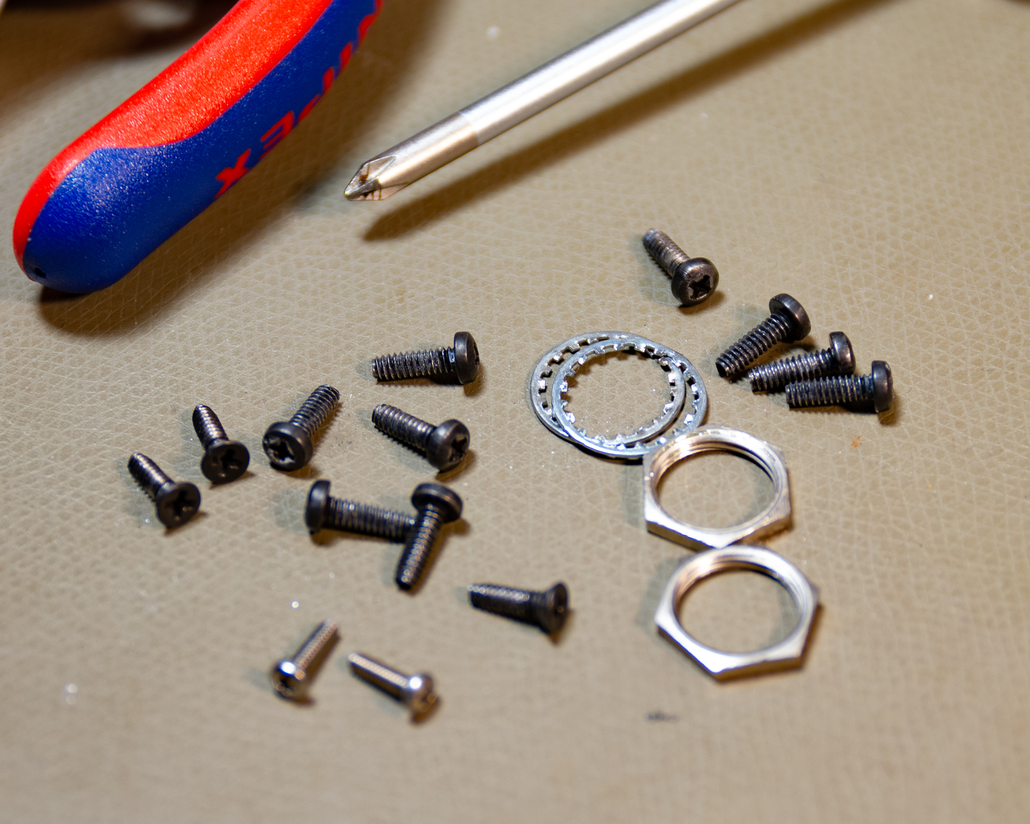
Disassembly is more involved than modern Behringer equipment, though not horrible either. The top lid is actually L-shaped, so you need to remove three screws on every side (front, sides, bottom) to release it. You also need to unscrew the SCSI2 connector and BNCs to get the cover off.
My assumption is that they designed it this way to simplify the sheet metal construction, the top lid can be manufactured quite easily with a bender, and the bottom and front panels are simpler than modern designs with a sliding lid.
They do get points for using all machine-screws, though most of the screws go into aluminium so don't over-torque them.
Internals
I took some pictures of the internals:
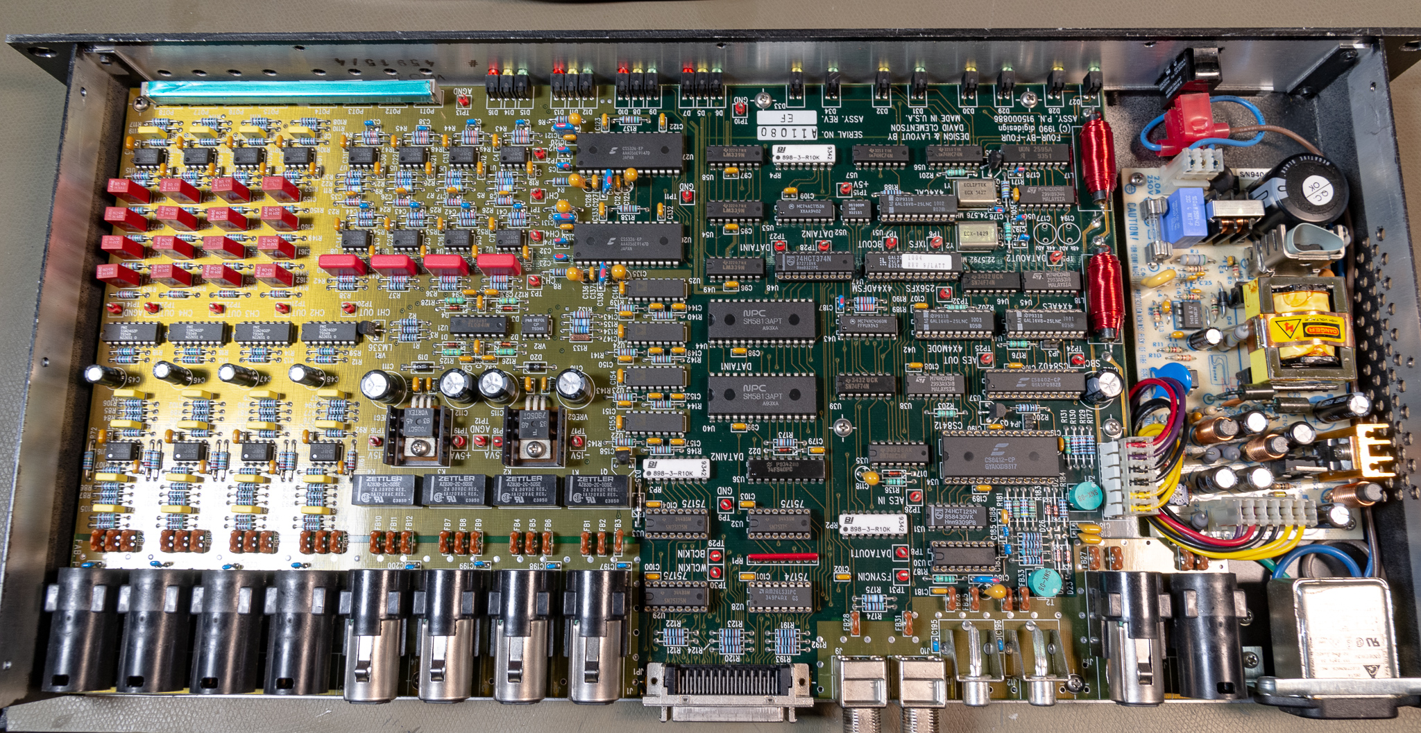
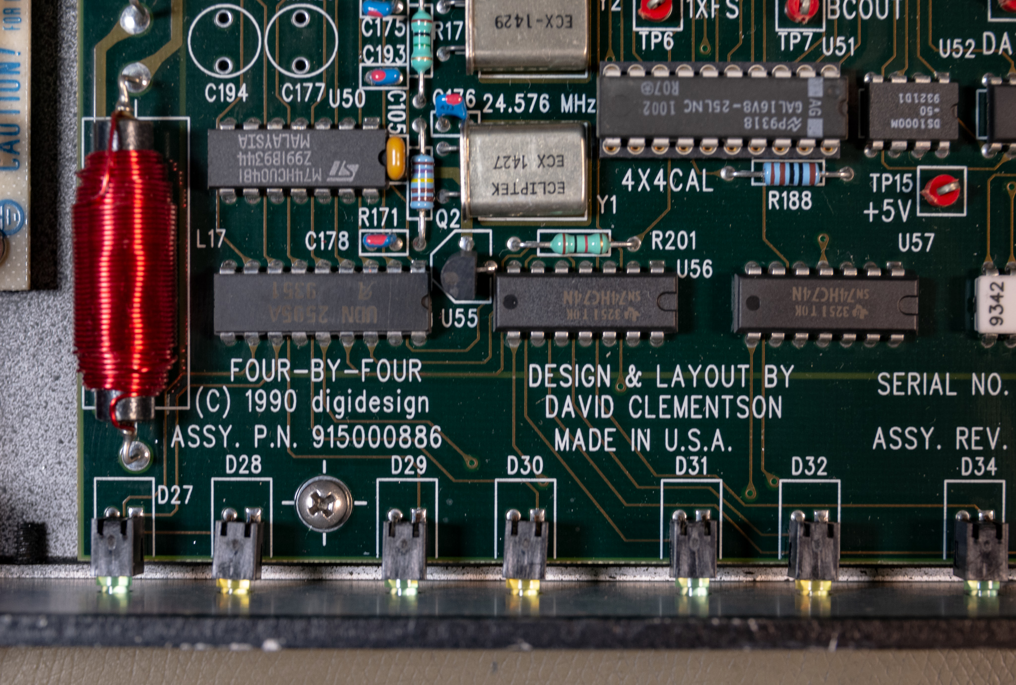
The unit is built on a single very large PCB (except for the PSU), it appears to be at least 4 layers. This is definitely a high end piece of kit (especially for 1990).


I'll try to describe how I think this worked in the next section.
Recap
Note: I replaced most of the electrolytics in the units before taking pictures. The power supply output capacitors had leaked and did cause some corrosion on the PSU, though no lasting damage.
Power Supply
The PSU is an off the shelf ±15 V and 5 V supply (Skynet SNP-3034, as mentioned above), the ratings are 5 V / 1.5 A, +15 V / 1.2 A, and –15 V / 0.3 A. It's a universal voltage input, no problem using it anywhere.
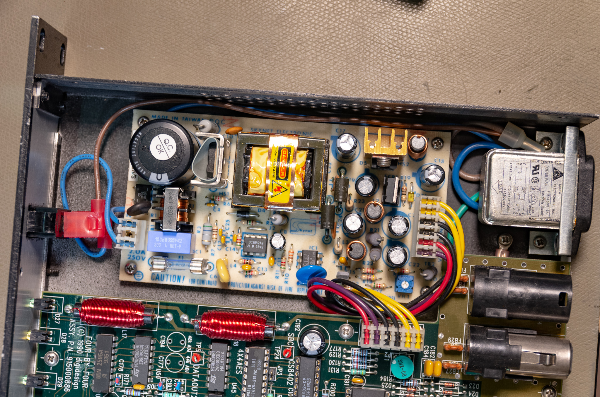
As mentioned, the output capacitors had failed in my unit, and leaked a bit. This caused some corrosion on the rectifier diode leads but no real damage. Being on a single sided PCB actually helped for one since there were no vias to damage. I do wonder if the electrolyte has soaked into the PCB substrate, since it still smells like electrolyte when warmed up.
The PSU was small enough that soaking it for 30 minutes in IPA in an ultrasonic cleaner was possible, this removed most of the corrosion and electrolyte.
The original capacitors were all Nippon Chemi-Con, so it does seem to be a bad batch or similar, not the result of cost optimization (it seems to be well built by power supply standards). To re-cap it, get a pile of 470 µF / 25 V (4⨉), and 1000 µF / 10 V (2⨉) capacitors.
I didn't replace the controller filter capacitor (the small electrolytic near the middle), nor the bulk input capacitor. These measured fine, and were clearly from a different series so no reason to suspect them.
A supply like this isn't particularly expensive, so I wouldn't advice repairing it if broken unless it proves very simple. Sourcing a new replacement shouldn't be a problem from e.g. Digi-Key, but you may need to replace the connectors. Something pretty close is the Cincon CFM40T-03 (note: different output pinout, may not have exact same screw hole pattern).
For some reason the wiring (made and designed in USA) uses Euro style colour coding for line/neutral (brown/blue), but the brown changes to blue after the switch. Strange, but not actually important (AFAIK you are not required to use standard colours inside non-serviceable devices).
ADC and DACs
ADC
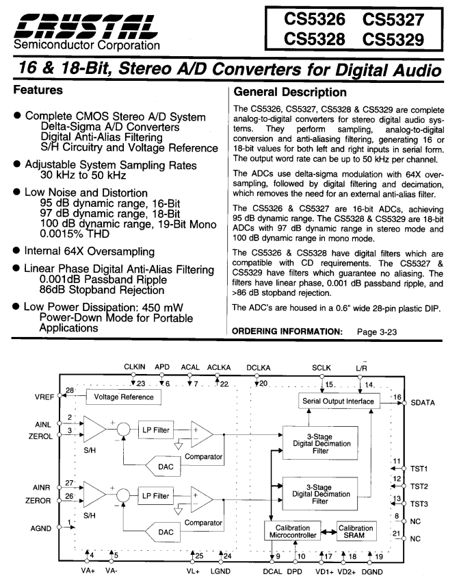
The ADCs are listed as 16 bit output (modern ΔΣ type).
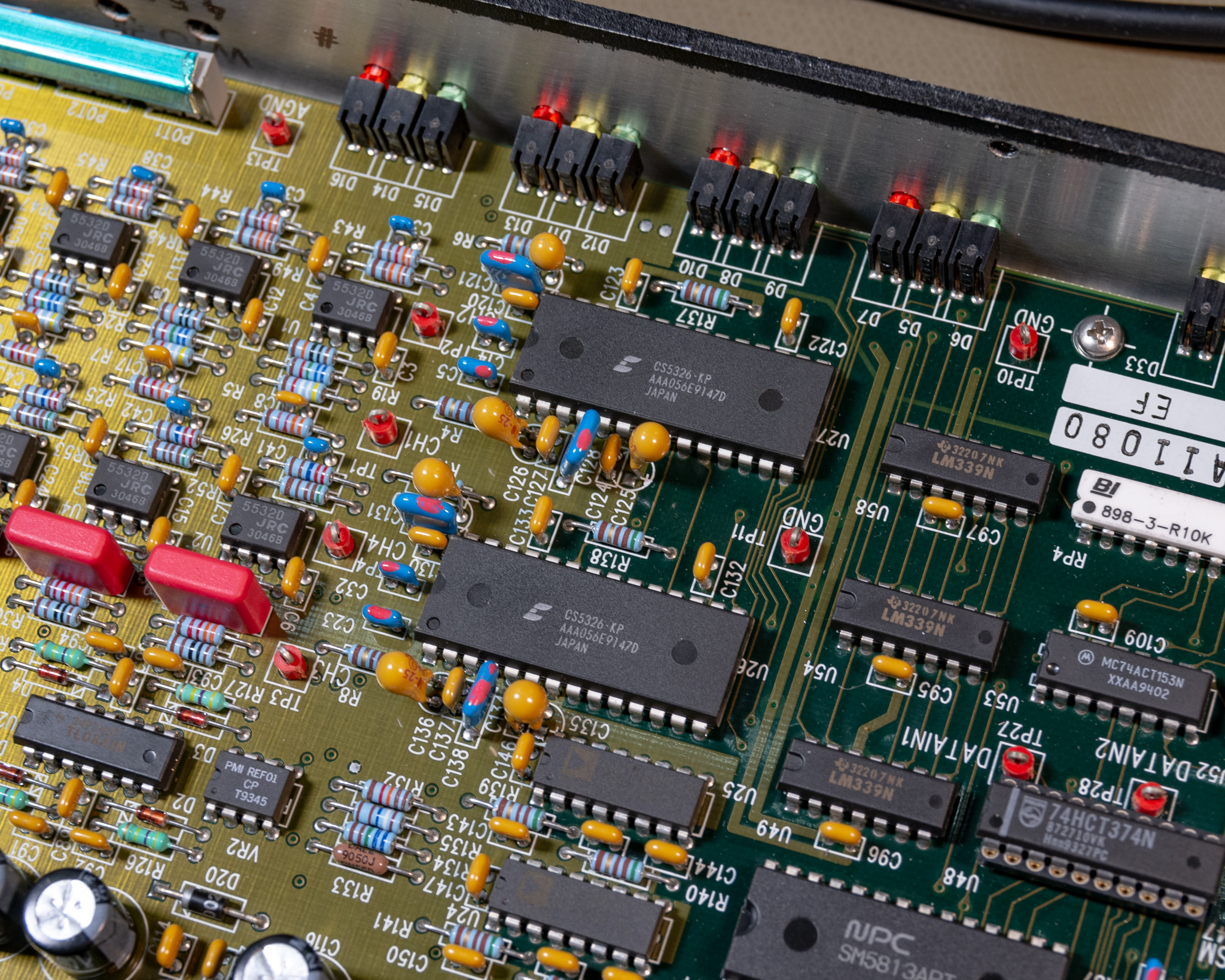
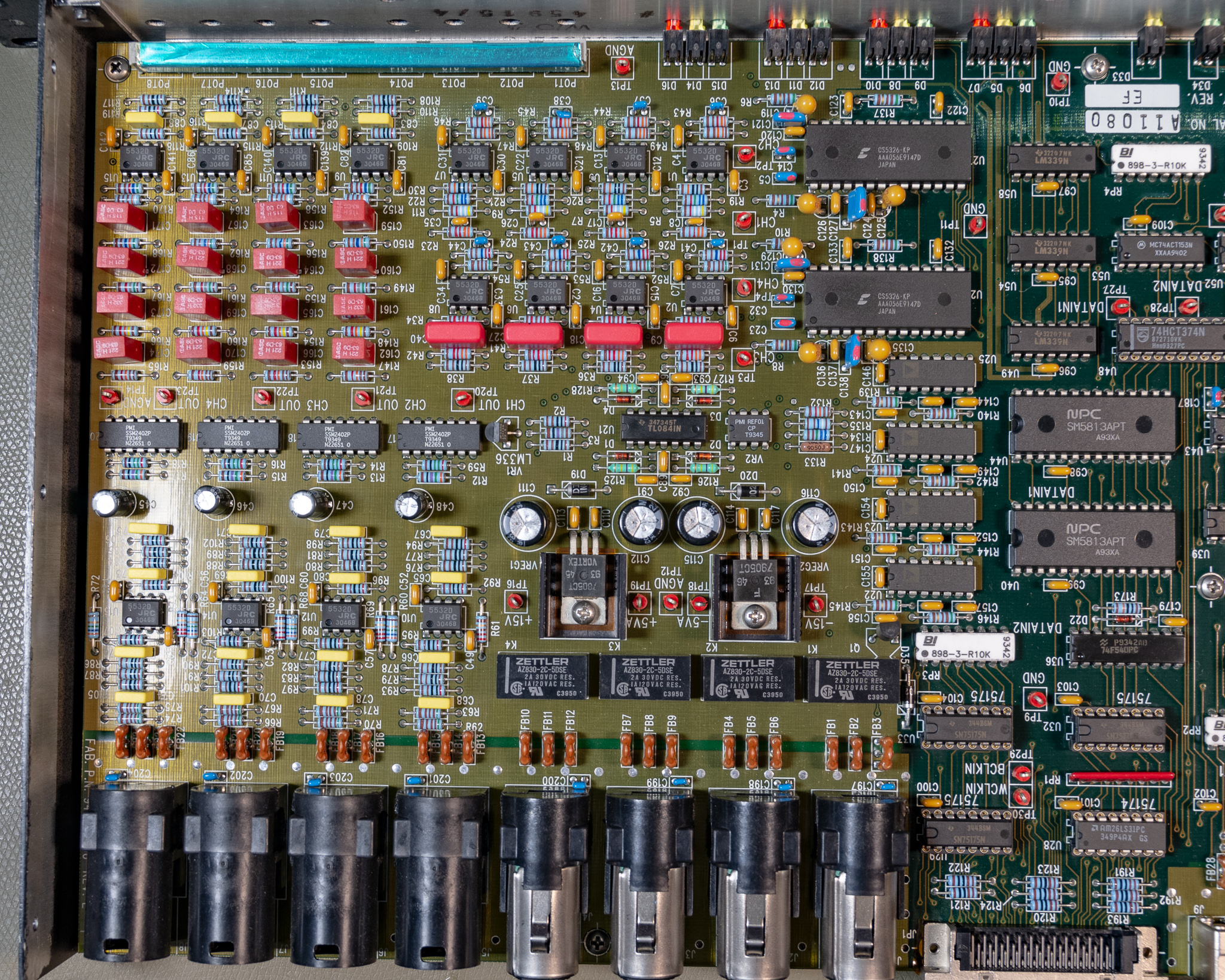
The device uses two CS5326 ADCs, which were fairly new when this device was designed, and appear to basically be equivalent to a modern 24 bit ADC except for the poorer resolution. They operate in the same way as basically every other modern ADC, though I believe this was a fairly new technology at the time.
This type of ADC uses oversampling, and therefore (as mentioned below) doesn't really require an anti-aliasing filter. A simple 1st order RC filter is perfectly suitable for this type of ADC (same goes for DACs). The 64⨉ oversampling used here means the nyquist frequency at the input is around 1.5 MHz, instead of 24 kHz.
DACs
The DACs are more interesting than the ADC, since they are not the same as modern systems.
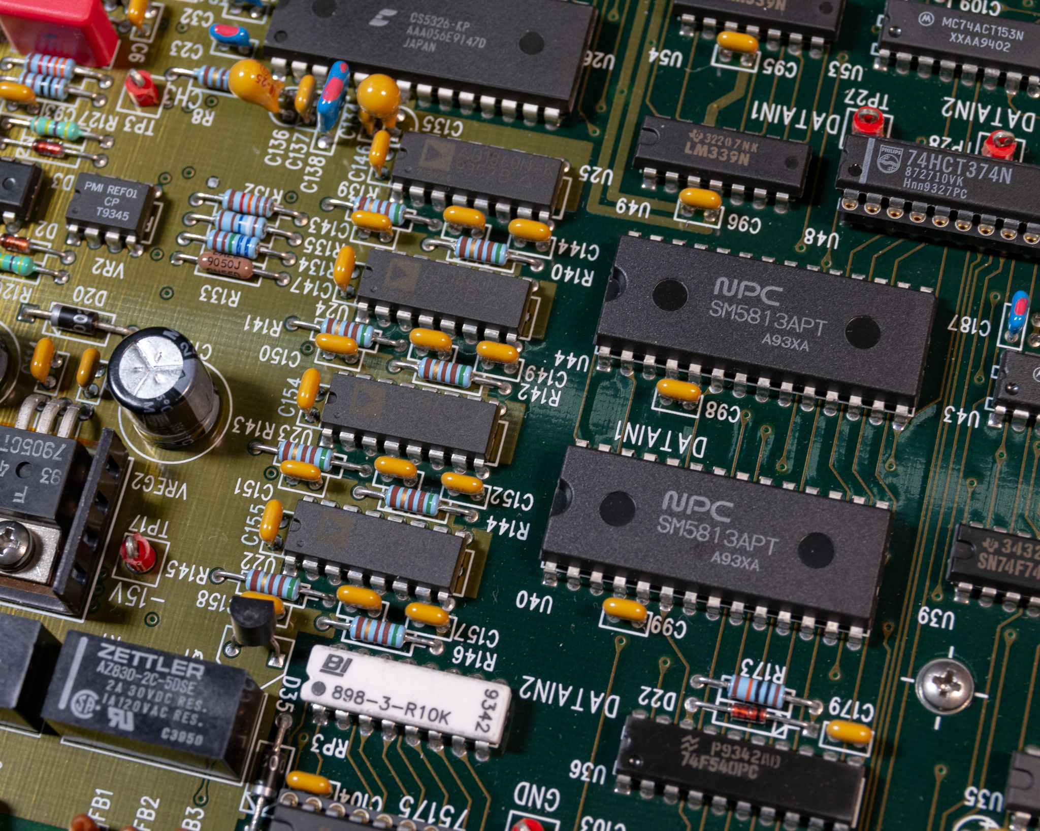
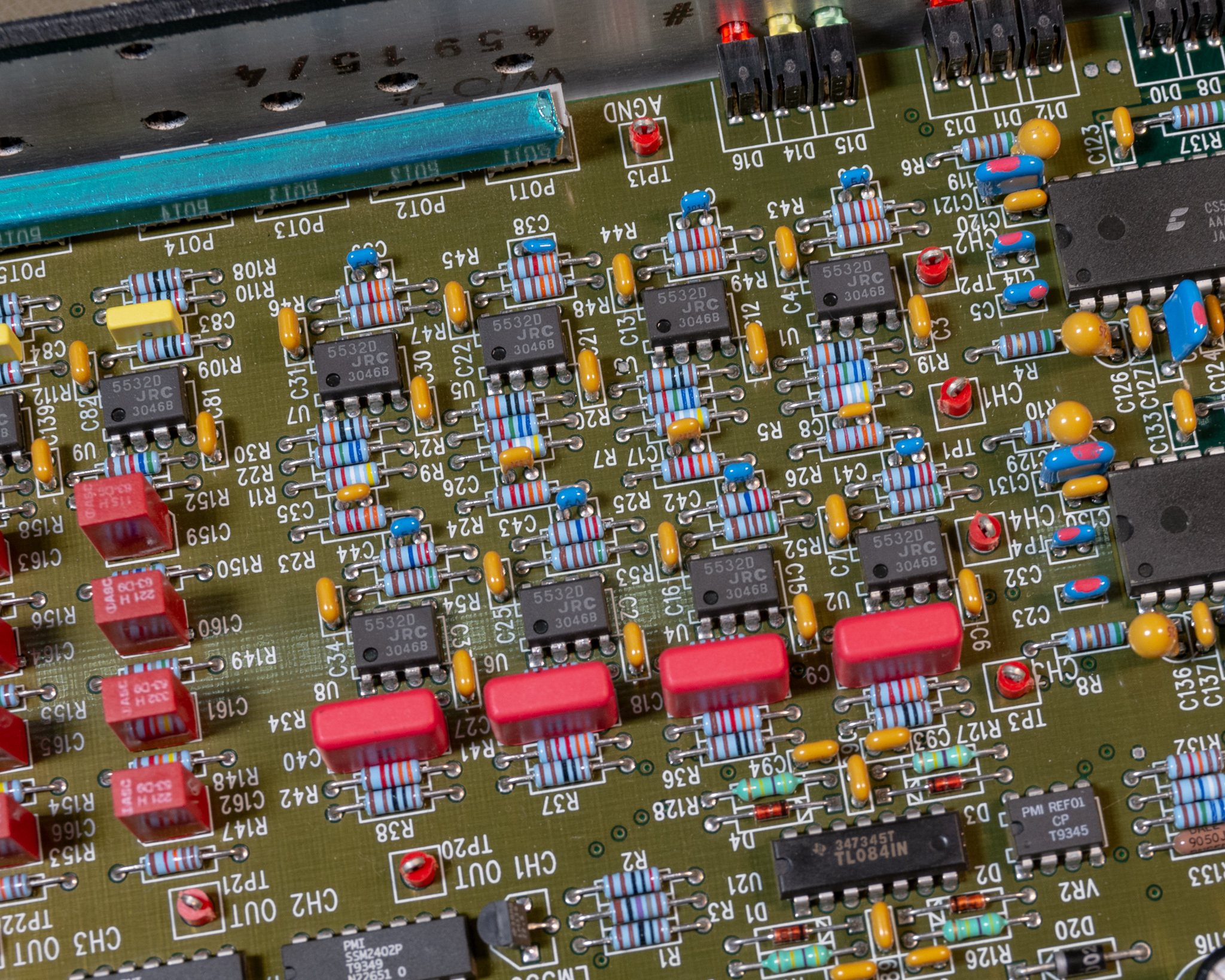
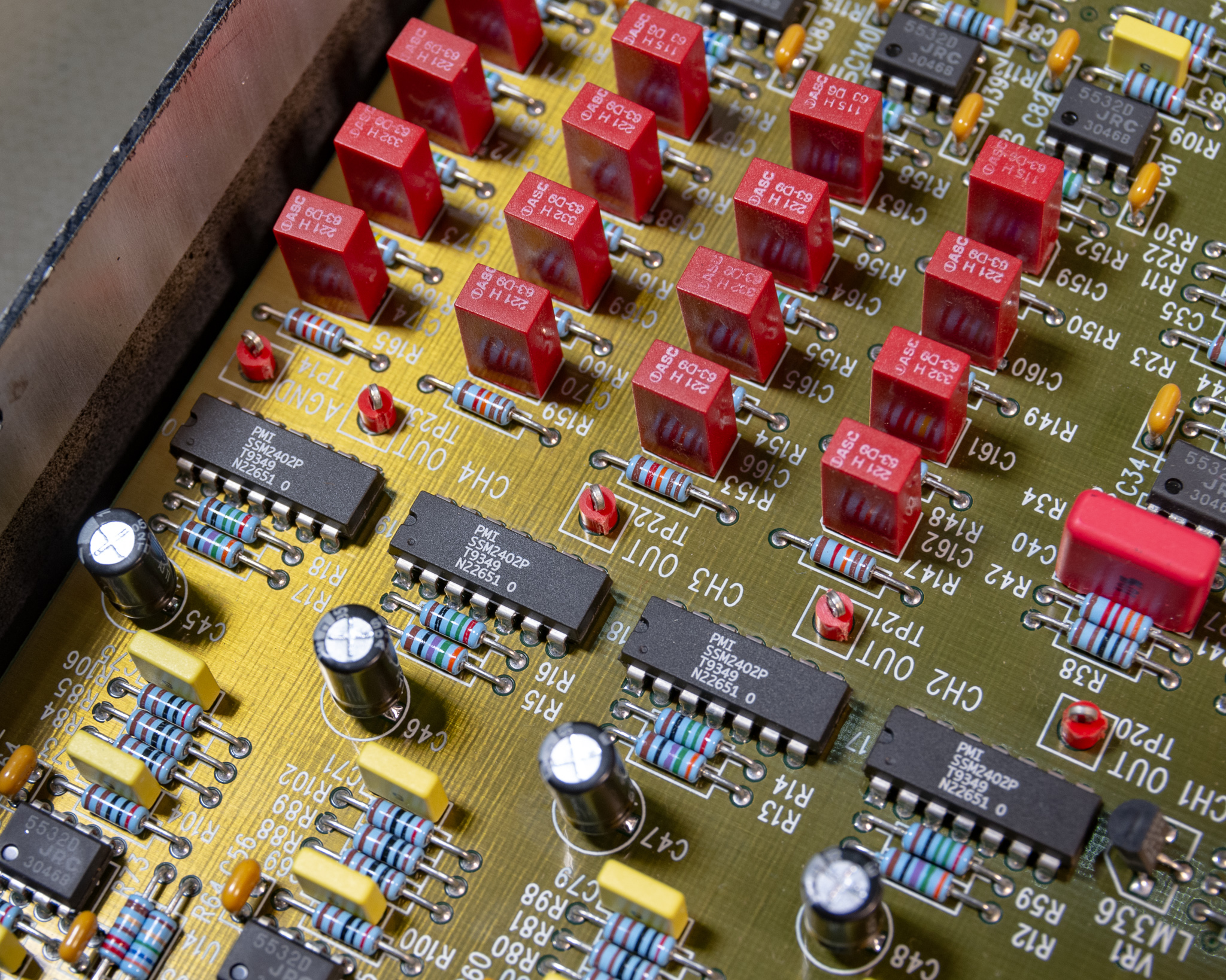
The keen eyed viewer will notice there are 4 DAC chips of type AD1860, and two ICs near them labelled SM5813. The SM chip is manufactured by a fairly uncommon name to see: Nippon Precision Circuits Inc. (NPC).
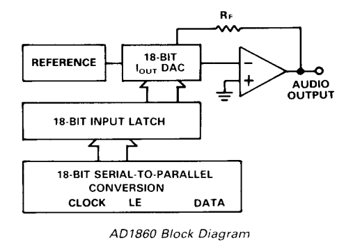
The AD1860 is an Analog Devices 18 bit audio DAC, no surprises there.
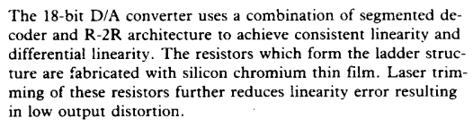
The R2R DAC is a simple DAC that's often built from discrete resistors where a real DAC is too expensive and you don't care too much about performance. However, it's a perfectly valid design to use for high performance, but I suspect it's a fairly complicated thing to get right and achieve good performance. This DAC is specified to have better than 0.002 % THD+N and minimum 102 dB SNR (A weight), which is quite respectable.
This type of DAC is rarely seen in audio applications today since ΔΣ DACs are much cheaper to build and offer very good performance. They do require a bit of silicon to perform the upsampling, which is possibly one reason it took a while to take off.
Oversampling
A key advantage of ΔΣ DACs is that they naturally operate at at least 64⨉ the sampling rate (typical 128-256⨉, sometimes up to 768⨉). (These systems also operate with a 1-bit resolution, and use an error-feedback system (the Σ part of ΔΣ), but that's a whole 'nother article).
The analog output will therefore be very clean, except for a lot of noise typically centered at a few MHz. Very simple 1st order filters are often used to remove this, and normally it won't be a major issue even if you don't (it is an EMI issue though).
Because this DAC is not oversampling, it would require a very complex high order filter to remove quantisation noise from the output. If this is not done, it could actually have a noticeable effect on the signal quality, especially if the input was digitised again. This was a major annoyance when CD players were introduced, as it cost money to implement this filter.
In theory, the filter to perfectly remove artefacts from a DAC running a 1x sample rate is infinitely high order (and therefore impossible to implement).
At one point someone came up with the idea of oversampling, and this was a very typical marketing trick used for CD players in the late 80s and 90s, initially 2, 4, and 8⨉ oversampling. Later with ΔΣ marketeers were overjoyed at the prospect of selling 256⨉ oversampling!
This idea is very similar, except in this system the resolution is not reduced like a delta sigma system. The principle is that an ASIC can take a normal digital bitstream, then increase the sample rate by some factor (e.g. 8⨉), then apply a digital low pass filter to the upsampled bitstream. The DAC can then operate at 8⨉fS, meaning the actual nyquist frequency of the output will be 8x higher, and the associated low pass filter can be a fair bit less complex.
Enter NPC:
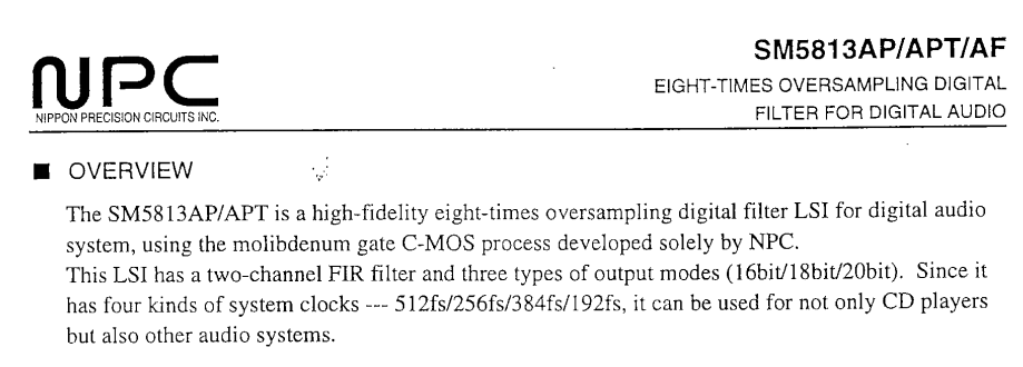
The SM5813 is a special purpose chip which accepts a serial bitstream, then upsamples the data, applies a FIR filter to it, then outputs it at the new 8x speed:
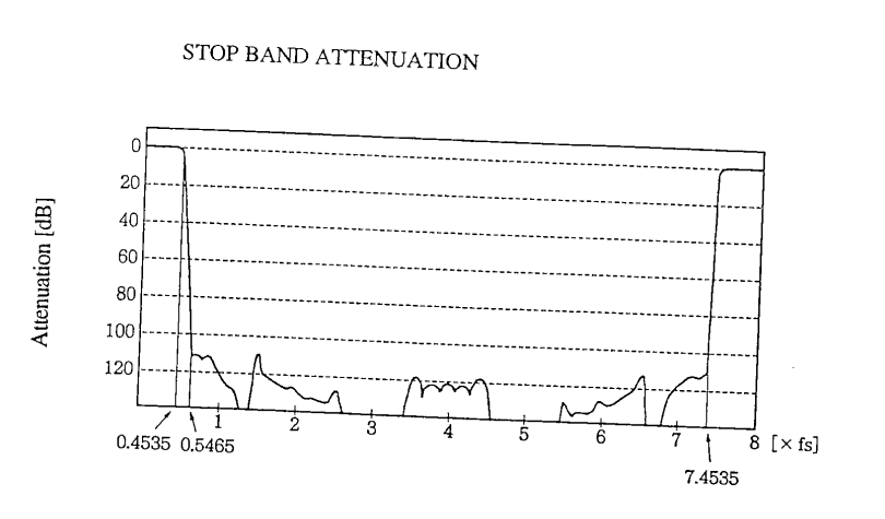
The filter is digitally designed and can therefore be significantly more repeatable, and cheaper. This type of filter plot is typically also found in modern delta-sigma DACs and ADCs, since the same principle is used, though for those systems there is also a resolution change.
The AD1830 is designed to operate in with a chip such as this:
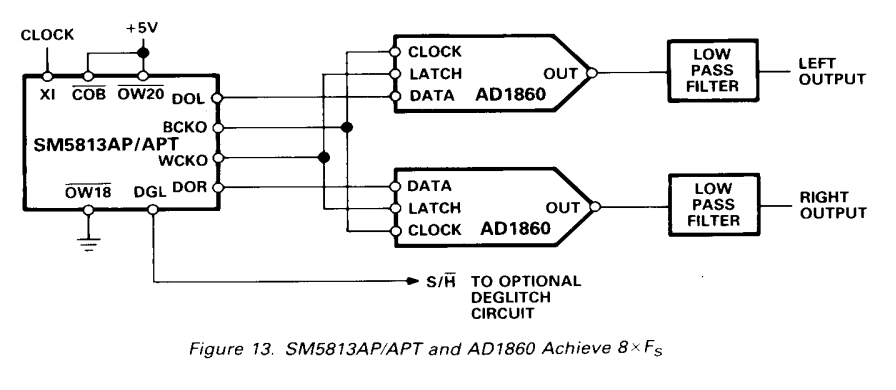
This combination was probably fairly common at the time, though I believe by the mid 90's the delta-sigma solutions were far more common.
Note: I'm not sure why these systems would use an 18 bit DAC when doing 8⨉ oversampling, if the oversampling ASIC did some noise shaping then the same performance could probably be achieved with a lower resolution DAC. Since the source data is 16 bit in most cases there's little benefit in going above this (except for cases where digital volume controls are used).
In the interest of remaining unbiased (read: extremely biased), I will note that some object to the use of digital filtering in the audio playback stream, pointing out the devastating effect of such interpolating filters on the signal quality.
Yet in practice there is no free lunch- all digital signal manipulation comes at a cost – musicality that is. Since part of the Delta Sigma conversion process (similar to switched power supplies) is a high frequency pink noise, it requires a lot of digital filtering or oversampling and noise-shaping. Essentially, oversampling is a corrective process, which needs to sort the digital data in the signal and come up with bits that are not are not a part of the original data stream. These bits is a missing information we do not have (not part of the recording), so they need to be invented (process called interpolation) and then noise-shape filtered. Noise-shaping and overs-sampling process are essentially adding artificial information (artifacts) not present in the original samples.
- DELTA SIGMA VS NON-OVERSAMPLING (NOS) R2R DAC DESIGNS (sw1xad.co.uk)
Note that this article is primarily about modern delta-sigma converters, the oversampling R2R DAC used here is an intermediate technology (which is probably also bad).
Also should note that while I do find audiophile stuff amusing, SW1X seems to be a company specialising in selling musicality optimised designs for audiophiles.
The products they make appear to be what they claim, and the market segment they operate in doesn't really care that much about measured performance or the science of signal processing.
Most audiophiles seem to be interested in the æ s t h e t i c s of the product, and that's certainly what they're getting.
Analog Circuitry
All the analog routing is on internal layers with a ground fill above it, this is perhaps not entirely necessary but it could provide a bit of shielding for high impedance signals.
Inputs
The input amplifiers are NJM5532 (JRC5532) dual low noise opamps, this opamp is the bread and butter opamp of professional audio, and is still manufactured and in common use. The same basic amp can also be sourced from other manufacturers including the NE5532 from Texas Instruments.
The specific NJM5532s used here are the "D" grade, which might sound bad, but actually sounds good, since those devices are a lower noise variant than the standard type.
A further digression is the "Equivalent Input Noise Voltage", which is guaranteed to be less than 1.4 µVrms for this opamp. Calculating nominal input noise voltage with 5 nV⁄√Hz and 20 kHz bandwidth yields 0.7 µVrms input noise. The deviation from average is probably affected by the 5 nV figure being nominal while the max noise figure is a maximum parameter. My calculation ignores the low frequency noise contribution as well.
Assuming a peak line level swing of ±10 V (7.07 Vrms), and that the amplifiers are operating in unity gain, this gives an amplifier SNR of: 20·log10(7.07 V ⁄ 1.4 µV) = 134 dB. As such, for (high) line level applications these amplifiers have plenty of margin vs. the ~90 dB SNR of the ADC, assuming the design is well implemented.
Note that this calculation also ignores resistive noise and the effects of current noise, which is typically relevant for e.g. differential amplifiers like this.
Another digression: These opamps were commonly used for RIAA (vinyl) preamps, in this case I do think they are a bit marginal. This is due to their high current noise (due to being bipolar), and high 1⁄f noise floor of around 100 Hz, expect a bit of rumble from preamps built like this. When measured with an A-weight filter, this low frequency noise is typically not relevant.
The OPA1642 is a far better choice for a modern moving magnet pickup, having slightly better voltage noise, a lower 1⁄f floor, and being a JFET input means no current noise. It's worth noting that in the 1980s the standard JFET opamp was the TL072, which is very (voltage) noisy by modern standards (around 30 nV⁄√Hz). Bipolar opamps were often the best choice then even though they aren't the best choice today.
Since this is a line level input device (and not a microphone preamp), the choice of standard opamps is perfectly reasonable.
The inputs are DC coupled with a DC servo circuit (and some kind of cleverness I haven't figured out yet).
The input stage is a standard differential amplifier, there is a DC offset servo seemingly using two opamps. The large red film capacitors are used for this function as the integrator element.
It seems the voltage reference (presumably the ADC reference) is divided down and used to set the DC operating voltage for the input stage, and as such all the input test points have a 200 mV DC offset. This seems to be intentional, and poking at it a bit confirms all the amplifiers are working in closed loop as intended.
The signal is routed through the potentiometers for level control, and applied to the ADC.
Note that there are a lot of labelled test points on this board, much appreciated.
There are some relays that look to be in the signal path here, not sure why those are needed for the inputs - could be for protection? It does not appear to be a bypass function.
As expected, there isn't much need for low pass filtering due to the modern ADC type.
Outputs
The output amplifiers are also NJM5532s, and it appears that (not unexpectedly) there is a fairly high order output low pass filter for the DACs.
The SSM2402 ICs are analog muxes designed for high level audio, and are presumably used for output muting. The signals also stop by the potentiometers on their way.
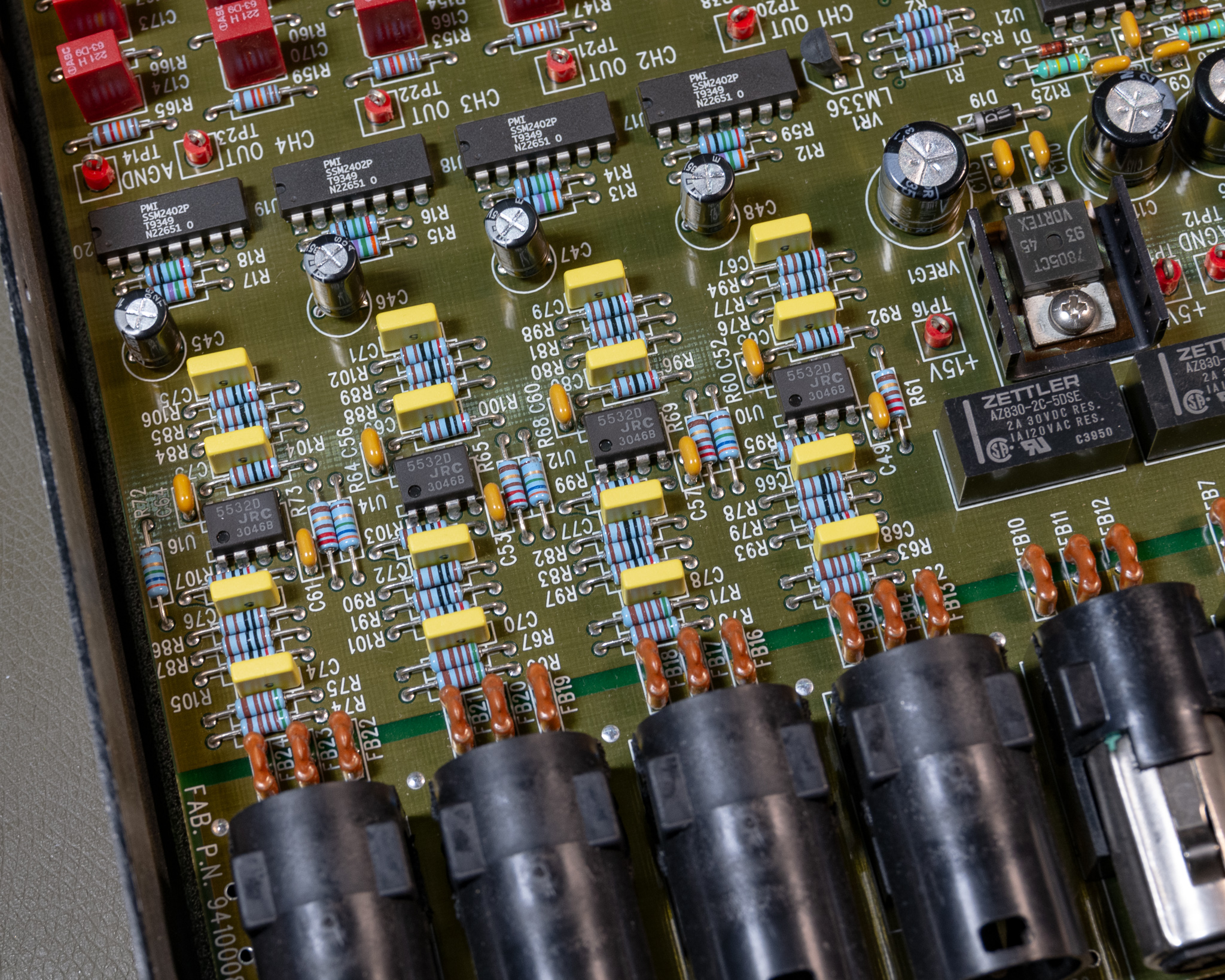
The output amps, are, surprisingly, NJM5532s. I haven't spent much time studying it, but seems to be a fairly simple differential driver with low output impedance and some low pass filtering.
Also note the filter-elements, these appear to be T-filters and they're used for basically all I/O except for the SCSI connector. A nice touch, probably helps a fair bit with EMI both emitted and applied. The series inductance is around 400 nH for these filters.
Filters like these are quite important when using bipolar opamps as input stages (or when you use protection diodes at the input), since strong RF (e.g. from GSM phones back in the day, or modern LMR/PMR two way radios) can be rectified in the input transistors of these amplifiers. Modern CMOS/JFET opamps are typically significantly more resistant to this issue, as long as you include at least an RC low pass filter on the input.
See Texas Instruments SBOA128A "EMI Rejection Ratio of Operational Amplifiers" and AN-1698 "A Specification for EMI Hardened Operational Amplifiers" for more information on opamp EMI resistance.
Digital I/O
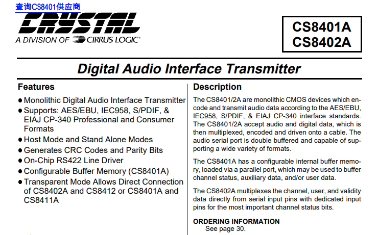
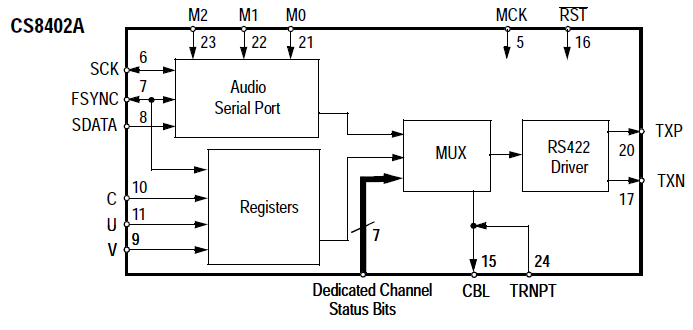
The digital I/O signals are generated using standard chips, the CS8412 is the receiver, and the CS8402 is the receiver.
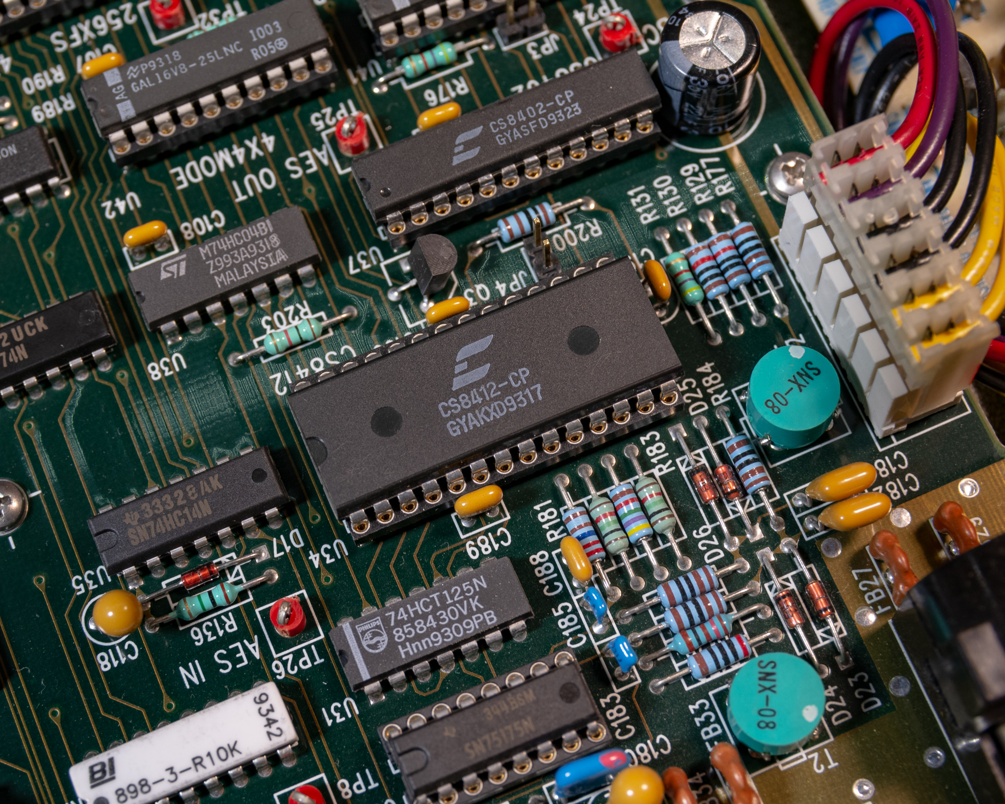
The AES I/O is transformer coupled, as expected. The S/PDIF interface is over standard RCA plugs and is not isolated.
The transmitter is fairly basic, and similar devices are still manufactured today, though you could do very easily with a modern CPLD (and it's often built in to audio DSPs) so I suspect the market isn't huge for these chips now.
The chip has a few different modes for e.g. consumer and CD mode (where a subcode can be transmitted as metadata, as well as professional AES/EBU mode.
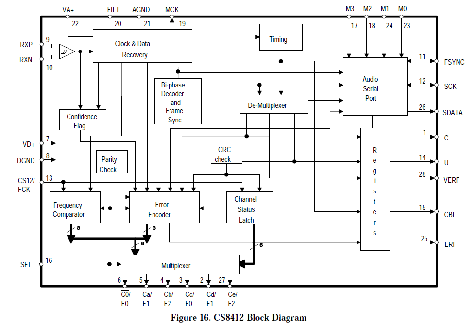
The CS8412 includes a PLL, which might be used as the system clock if the device is set to use it. Otherwise, the external device would have to be phase locked to the audio interface (e.g. through the digital out port).
Modern high systems based on e.g. the Analog Device SigmaDSP series typically include an ASRC that can convert completely asynchronous sources to the system clock without any special synchronisation.
Clocking
The system supports 44.1 and 48 kHz operation, and it seems to support this by using two different crystals.
The crystals are 512⨉fS, so they are probably divided by 2 (doing this is fairly common as it makes the duty cycle more predictable).
U46 is a 74F74 which is probably the clock divider. U50 is probably the oscillator (amplifier/inverter), it's a 74HCU04, a moderately uncommon unbuffered 7404 inverter (unbuffered inverters don't include a buffered output, making them a bit faster).
For reference, 512·44.1 kHz = 22.5792 MHz (⁄2 = 11.29 MHz), and 512·48 kHz = 24.576 MHz (⁄2 = 12.288 MHz). Aside from replacing the opamps with fancy variants, an audiophile may want to get TCXOs or similar to replace these crystals, these frequencies are still very common so shouldn't be a problem.
I'm not entirely sure, but it seems logical to assume that there are some restrictions on clocking this thing, since I don't see any ASRCs (Asynchronous Sample Rate Converters).
I assume that this device is designed as the clock source for most cases. The AES receiver can generate a clock output at the correct frequency, so it seems likely that this will be an acceptable clock source.
In any case, I don't see any way this thing can handle two separate clock domains, everything must run in sync. The choice of 256⨉fS for the BNC plugs makes sense in this context, since that frequency is the same as what the crystals generate, and when operating with external clocking everything probably runs directly off that clock.
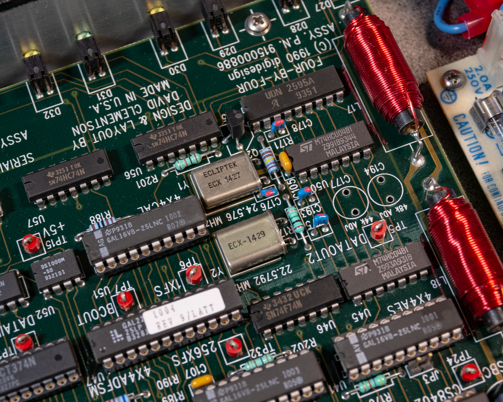
C194 and C177 are trimmers for the crystals (not fitted); I did some testing and 5 pF seems to be a suitable trimmer capacitor value (i.e. 1-5 pF or similar). However, there's no real benefit to trimming these. (If you care about the precision of your audio clocks, you should be phase locking them to a common precision reference anyway).
External Interface
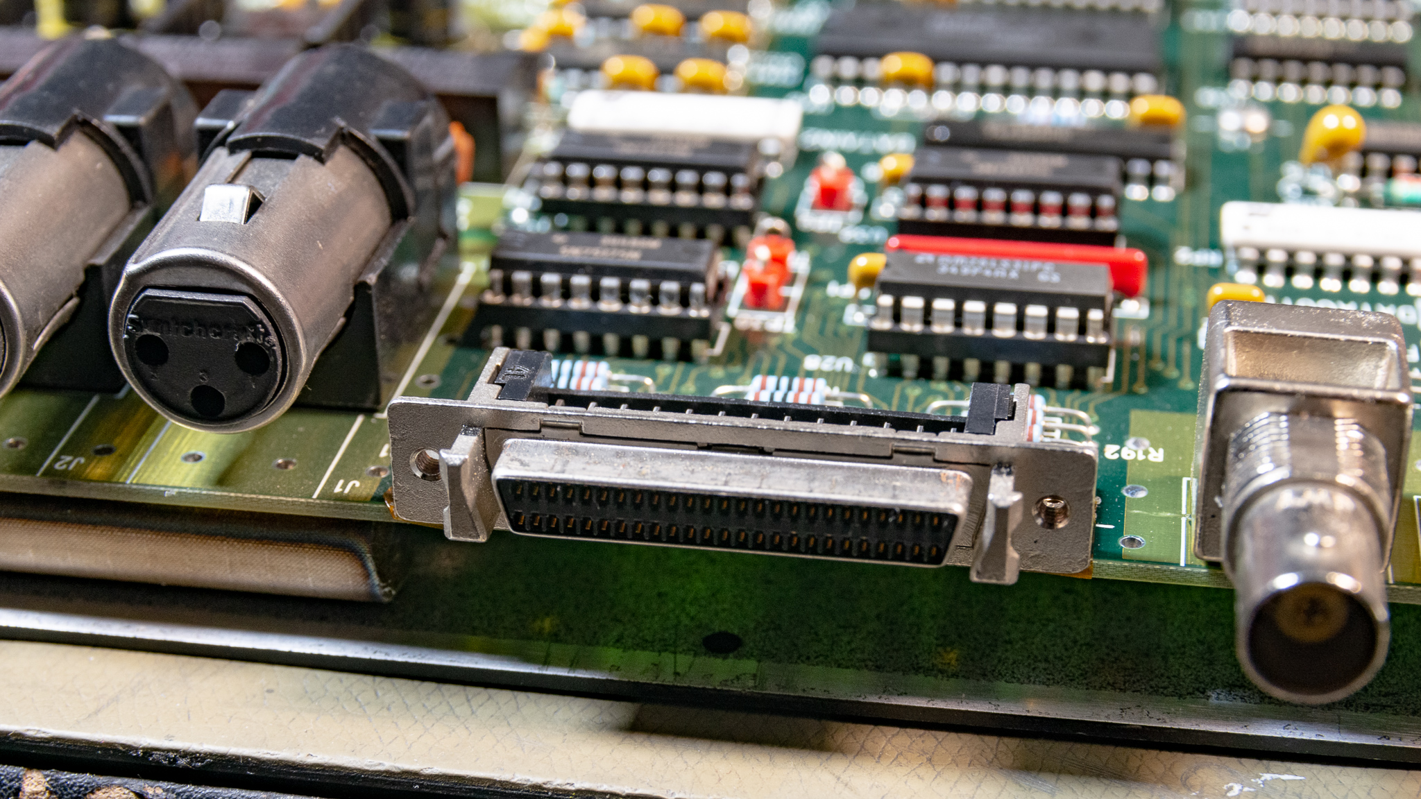
The external interface is as mentioned a SCSI2 high density 50 pin connector. This connects to the special DSP card that drives it.
The signalling format appears to be standard RS-422, and the signals appear to be a set of discrete signals, and a set of I2S/TDM like signals. This is fairly industry standard, though the connector choice etc. is proprietary. While SCSI2 cables aren't sold at grocery stores anymore, they are fairly readily available so not a terrible choice in hindsight vs. requiring custom cables.
Powered up, the device did appear to operate somewhat standalone, and the ADCs appear to be active by default. Applying signals to the inputs I could see the digital bitstream responded to it.
Other Notes
There are a few GAL chips, but otherwise the device is all off the shelf ICs.
The overall construction appears to be of excellent quality, many ICs are socketed in turned pin sockets. I haven't found any traces of rework or mods of any kind, which is quite impressive for something this size.
It's a fairly densely packed board, so routing it must have been a challenge, hats off to David, who put his name on the board: