Basic RF Over Fiber Laser Driver

One of the issues with building an RF Over Fiber system is the lack of affordable transmitter solutions. While detectors are extremely cheap, the transmitters can cost hundreds of dollars on the used marked.
Pre-made solutions can be found in the CATV marked, though performance here is often limited to TV bandwidths or around 40-800 MHz. In addition, there generally aren't as many full bandwidth transmitters in existence, the most common type of device is an active receiver with a return channel laser transmitter. These devices generally only offer around 50 MHz bandwidth, which is not great.
This type of architecture is one reason why cable internet generally has poor upload speeds, as only a small fraction of the possible bandwidth is utilized on the return path.
Pre-made high bandwidth transmitters can be found but not all that often, Ortel manufactured (still do as well) a number of very good high bandwidth transmitters in various shapes and sizes.
I've built a software controlled solution in my HFoF antenna project, but for projects with a lower integration level it made sense to build an analog regulator and house it in a standard die-cast enclosure.
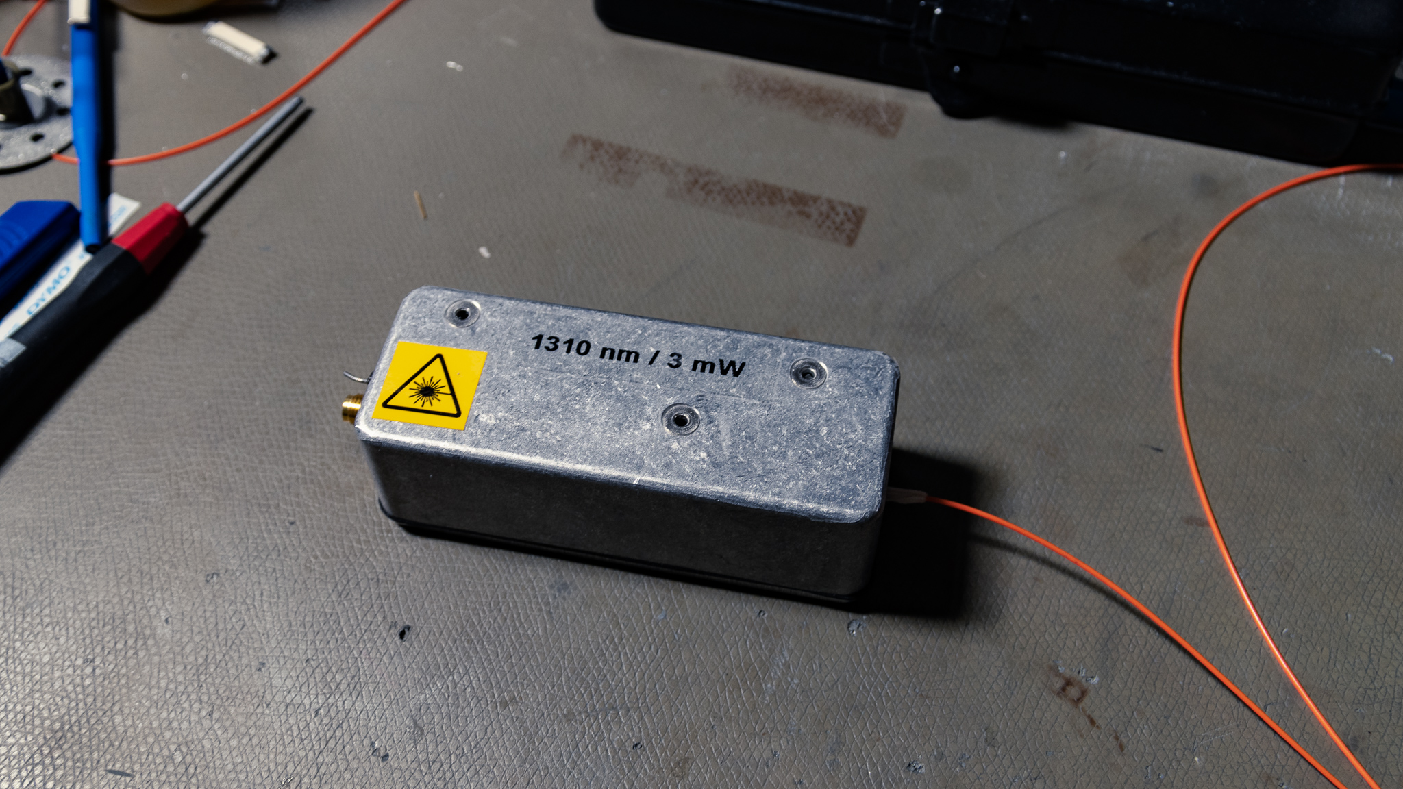
This solution assumes you found a decent source of cheap fiber coupled lasers, having a standard DFB/FP laser diode it's fairly simple to construct a functional regulated laser driver. These are available new on AliExpress, though you can also find good deal on eBay if you know what to search for.
The basic parameters of a typical 1-4 mW 1310/1550 nm fiber laser is:
- Threshold current around 8-10 mA
- Nominal current around 25 mA, up to around 70 mA at high temperatures
- Forward voltage around 1.7 V
- Around 200 µA monitor photodiode current at nominal power
The most common configuration is a positive chassis diode in a 4-pin TO package, with a floating monitor-diode.

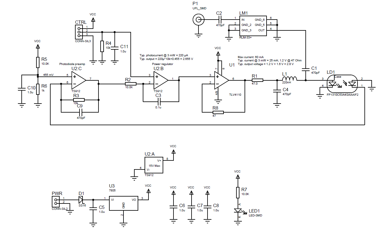
To implement an analog driver we want to control the laser current until the monitor photodiode current is what we want. This will effect a constant power regulator, which is generally a pretty good way of driving a laser.
The regulator scheme shown below uses a standard TS912 CMOS opamp as the amplifier and regulator. U2:C is the monitor amplifier, configured for a gain of 10000 V⁄A or 10 kΩ. This will amplify the nominal 220 µA monitor current of the diode to around 2.2 V. To avoid issues near 0 current/voltage, the positive input of the amplifier is biased to 0.455 V; this offsets the output of the amplifier as well so our target voltage for nominal power is around 2.7 V.
U2:B is the power regulator, this is a basic integrator which compares an external potentiometer with the amplified monitor current. The output voltage of the regulator is buffered in U1, which is a high output current opamp. A simple emitter-follower transistor stage could also be used here to increase the positive output current of the regulator without needing a specialty component. Since the system is closed loop power controlled, any voltage errors here are automatically corrected. If you're driving a higher power (e.g. OC-48 style) laser you may need more than 5 V supply as well, and the TLV4111 is a 5 V max part.
The buffered output voltage runs through a current limiting resistor R1 sized to limit the maximum current possible through the diode to less than the absolute maximum diode current. This resistor also isolates the buffer amplifier from any output capacitance, improving stability. R8 is not required, and is basically acting as a jumper to avoid having a via in the PCB layout.
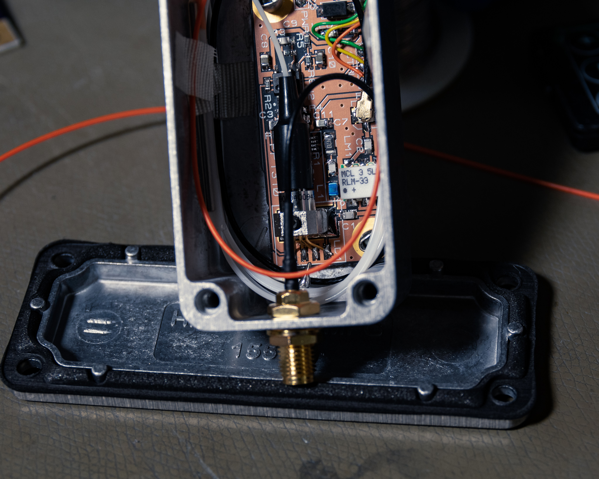
L1/C4 effects the bias-tee, and provides the DC path through the laser diode. The RF signal is applied to P1, and passes through a RLM-33+ power limiter device before being AC coupled onto the laser. The limiter is not absolutely required but makes the device significantly more robust, both against over-driving the laser, and ESD.
Diode clipping (last resort) or discrete PIN diode limiters can also be used, for pure ESD protection a varistor may be the most appropriate device.
One possible improvement would be to bias the anode at a fixed AC decoupled voltage, and apply the RF and DC bias to the cathode instead, this could reduce the effective diode capacitance and allow improved bandwidth. This would invert the polarity of the feedback loop, but would not otherwise require any major redesign.
Testing with a passive PIN detector indicates this implementation is usable up to at least 1.5 GHz, and is likely acceptable up to around 2 GHz, given I used a laser designed for 1800 MHz operation. The addition of a series resistor to the RF input may improve the input SWR of the RF port, potentially improving frequency response somewhat.
The above circuitry was implemented on a small PCB designed to fit in the lid of a Hammond 1550WA enclosure, though I ended up installing it in the box itself to make for a more rugged assembly.
The 1550WA enclosure is easily machined using basic hand tools. To locate the PCB I used a transfer punch, going one hole at a time. This technique allows for very precise location of holes without e.g. a coordinate table on a milling machine, though it's a bit slow.
The PCB and 7805 regulator are held in place using countersunk steel 3.2 mm pop rivets, this technique gives a highly repeatable holding force and no risk of screws coming loose. The 120° countersinking on the rivets is well suited to relatively thin walled parts. After labelling some 3M Tartan clear tape was put over the top of the box to provide some level of waterproofing and protect the labels. RTV silicone glue could be used to further waterproof the rivets if required.
An even better way to waterproof the rivets would be to use closed end rivets (DIN 15973 or similar) with some Loctite 577 applied.
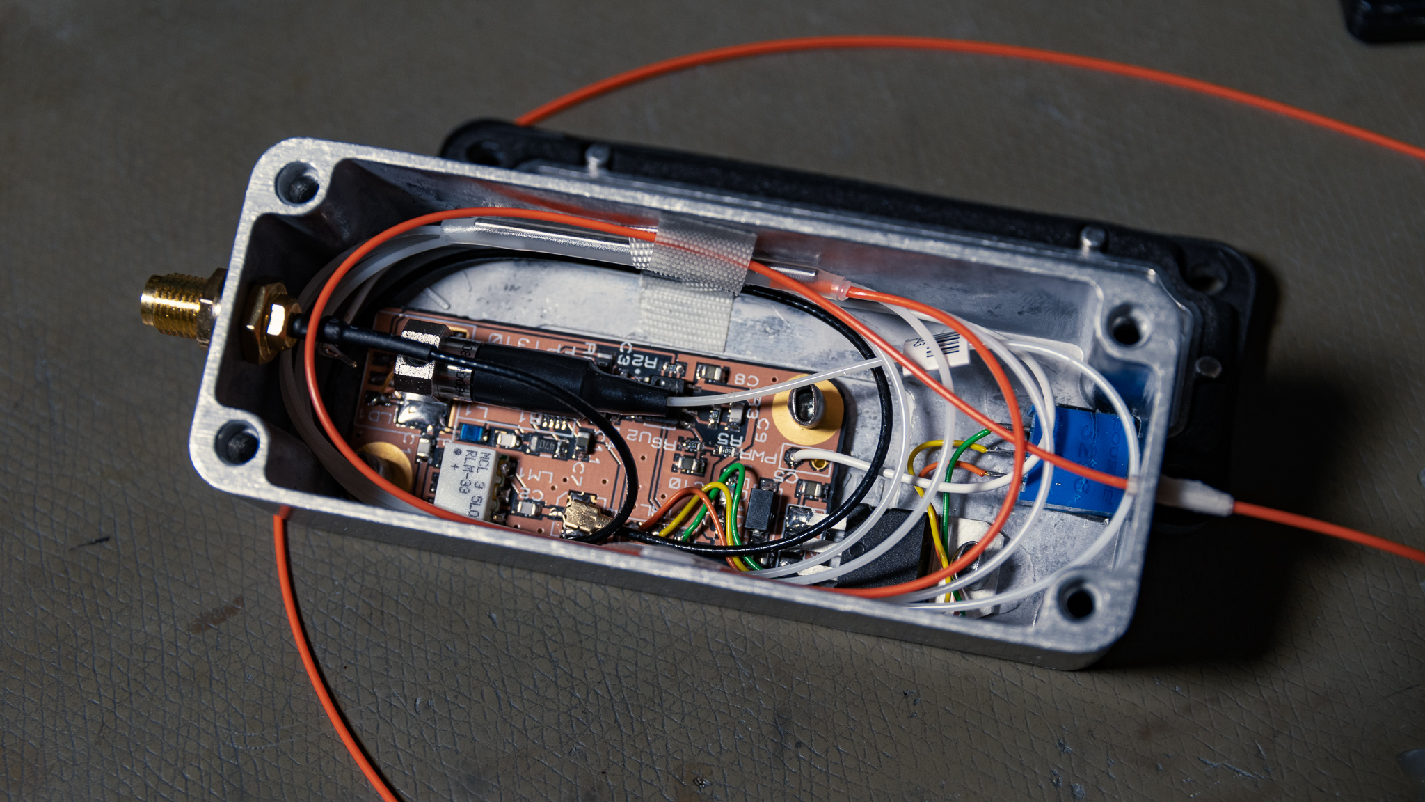
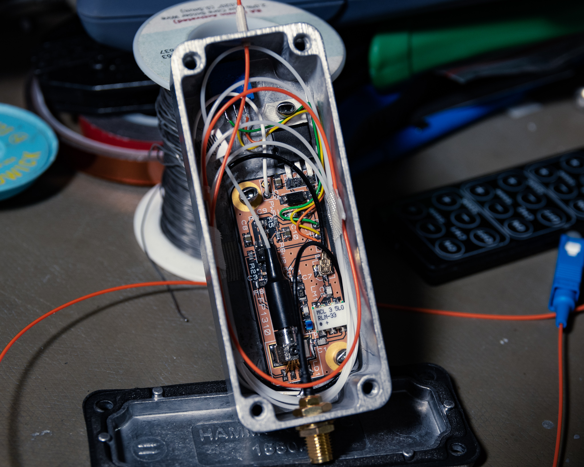
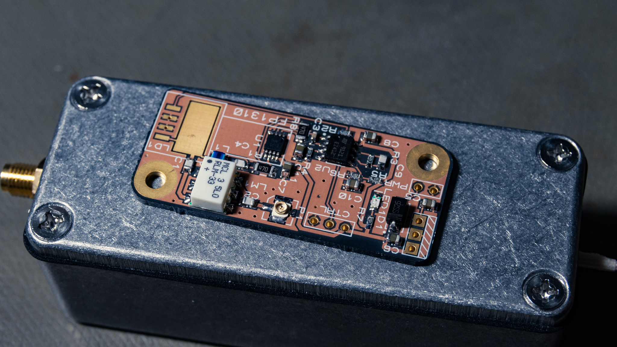
The PCB bottom layer is all ground fill except for the plated through holes, these areas were masked with polyimide tape before installation. The potentiometer is held in with VHB tape.
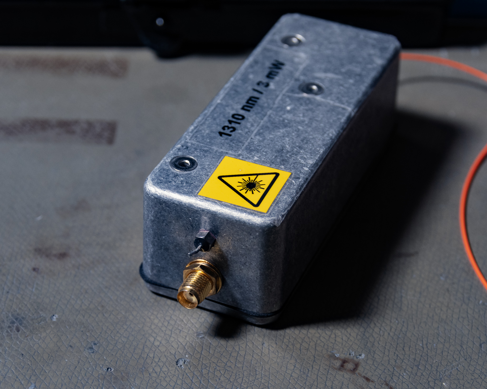
Power input is via a M3 threaded feed-through capacitor, and ground is via chassis/coax shield.
The SMA connector is a low cost pre-made SMA to U.FL adapter cable.
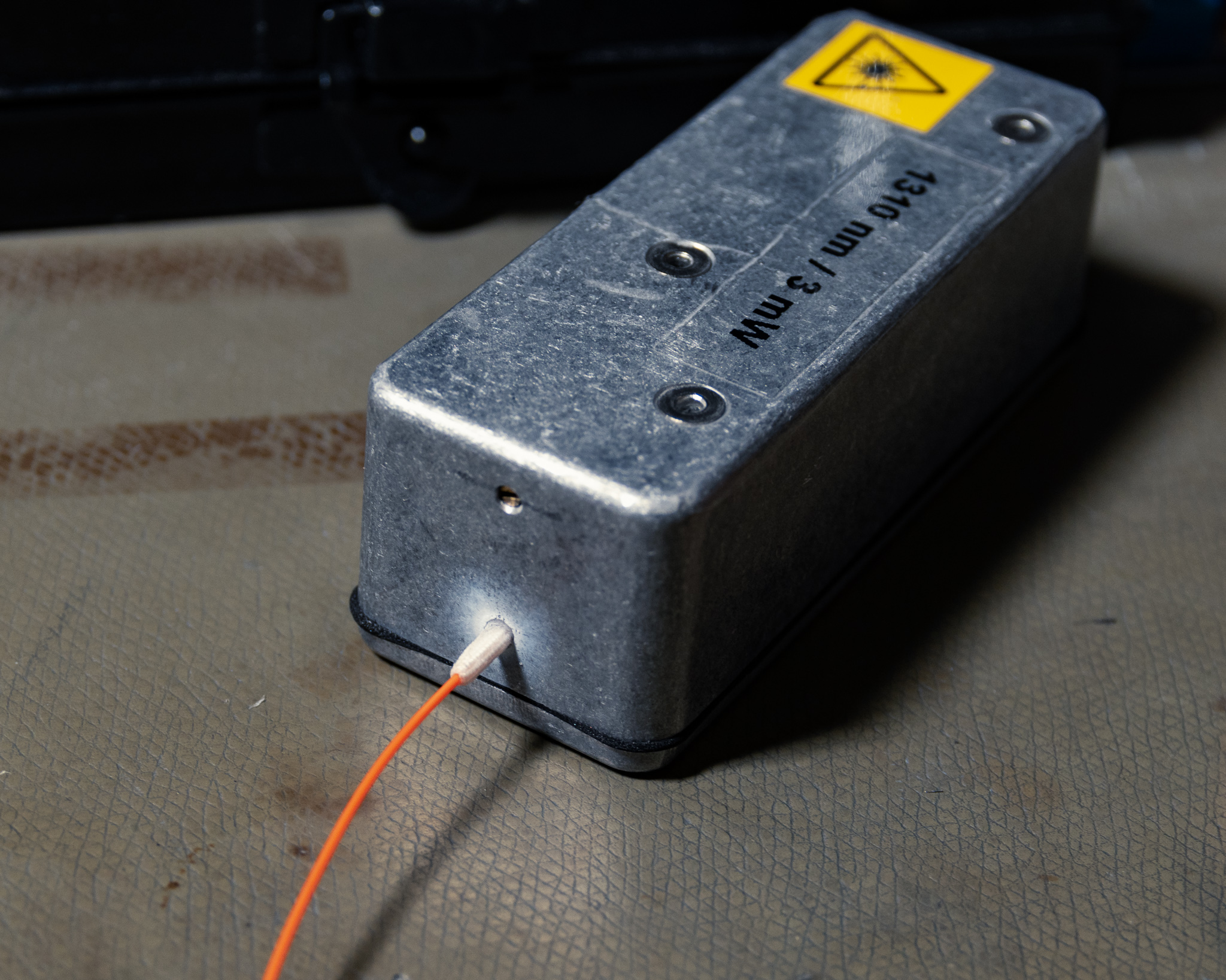
The fiber output is fed through a 2 mm hole in the box, in order to do this the original laser connector is removed and a pigtail connector of the suitable type (generally SC or FC in my case) is pulled through the hole and spliced in with a fusion splicer. The actual fiber feedthrough is done by wrapping a few turns of 69 tape around the fiber until it just barely fits into the hole. Then I soak the tape with 401 super glue to stiffen it, this is why there's a white flash near the tape on the outside of the box.
Keeping any holes in the box small helps with RFI protection, though this is more important when making active receivers than for transmitters.
The fiber and other cables are looped inside the box and held in place with 3M 69 tape. While the radius of the fiber bends is not entirely to spec for G.652, no loss of power was observed before/after the bending so it seems this is acceptable.
The laser I used for this project came with a machined mounting block that held the laser in with a tiny set screw, this block was cut down with a cut-off wheel, then soldered to the large laser anode pad on the PCB. The laser was then installed and the leads were soldered down and trimmed. This method worked pretty well, and avoids complicated mounting methods with screws etc.