BFU550X Based TIA Performance Characterisation

This is a followup to the previous ADF antenna system article, and details performance measurement of the BFU550X based cascoded TIA.
Table of Contents
Design Overview
TIA Basics
A trans-impedance amplifier (TIA) is a current to voltage amplifier, in electronics terms this is usually shown as an inverting operational amplifier, with the source-resistance set to 0 Ω. This in principle increases the voltage gain to infinity (for the case of a 0 Ω source impedance voltage source), but when a current-source is connected it makes sense again.

The output voltage is then set by the input current, and since the input signal is a current in Amperes, and the output is voltage in Volts, the gain unit is V⁄A. This happens to be equivalent to Ohm (Ω), and the gain is therefore often expressed in this way.
A TIA then has a gain unit of Ω, and since it's a current input amplifier, the noise performance is normally expressed as an input referred current noise density with unit Amperes per square-root of bandwidth. This mode of measurement is useful since it eliminates the bandwidth dependency by normalising it to 1 Hz. RMS noise (for white/thermal noise) follows the measurement bandwidth — increasing with the square root of the bandwidth — and this represents that fact.
TIA's are very commonly used in sensor applications, most commonly photodiodes, whose output is a current corresponding to the input optical power. Basically they give you one electron per photon – the gain unit is A⁄W. PIN photodiodes are standard for optical communications (APD's are better but harder to use and expensive).
PIN diodes require a 5 V reverse bias to achieve optimal performance, and they therefore have a fairly limited output voltage range if simply connected to a resistor; the DC component of the output current will quickly reach a significant voltage if a high value resistor is added. TIA's are used to effectively short circuit the diode.
TIA Design
The design under test today is a cascoded bipolar design, intended for use with PIN diodes in optical communications. The design can therefore make some assumptions about the signal, simplifying biasing.
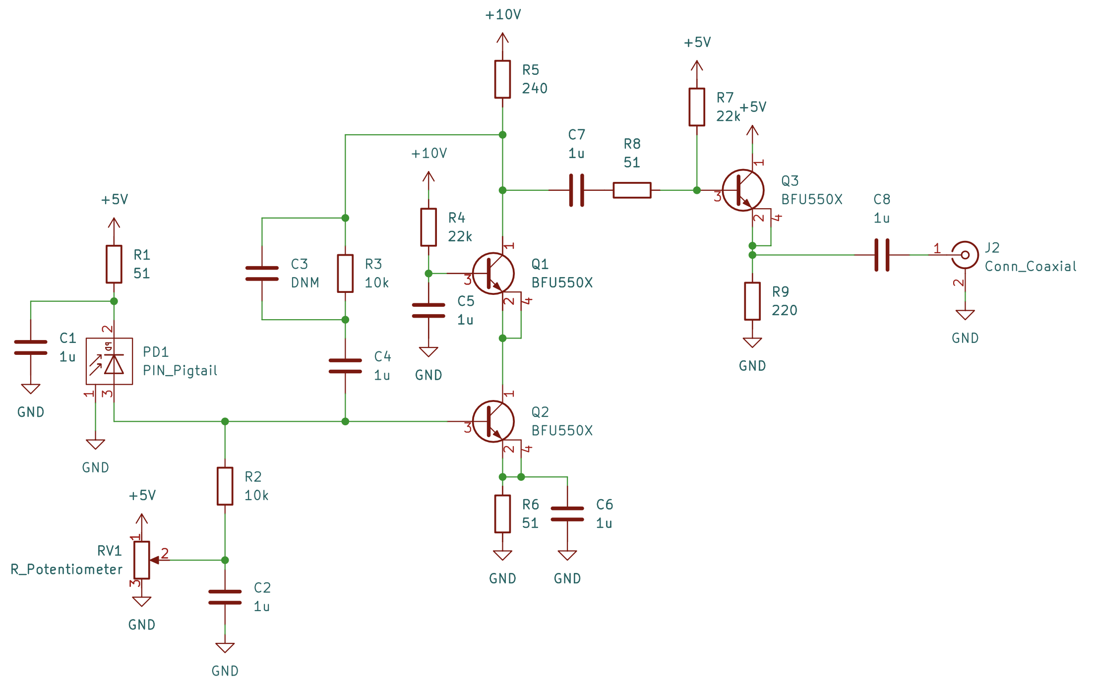
BFU550X high speed Silicon NPN transistors are used in this design, this is somewhat a compromise solution since MOSFET amplifiers generally have better current noise performance. However, good MOSFET amplifiers are getting harder to find as discrete devices, in particular dual gate MOSFETs are basically nonexistent in the market now.
The input current is generated in PD1, which is reverse biased to around 5 V to lower the diode's junction capacitance. RV1 is used to bias the amplifier, this design is relatively tolerant of variations in DC current level, but the assumption is that the average optical power to the PIN diode is constant. Therefore, the average DC photocurrent will be constant, and adjustment is not required.
Additional stabilisation is effected by using R6 as emitter-feedback.
Q1 is the cascode transistor, this operates as a common-base amplifier, ensuring that the emitter voltage is fixed. The effect of this is that the collector voltage of Q2 is fixed, meaning that the miller-capacitance from collector to base is eliminated. Ordinarily due to the voltage gain, the effective collector-base capacitance is multiplied by the voltage gain of the amplifier, limiting bandwidth.
The amplifier gain is set by R3, which provides AC feedback to the input. An emitter-followed output driver is included as well, this isolates the amplifier core from the output loading, and reduces the output impedance.
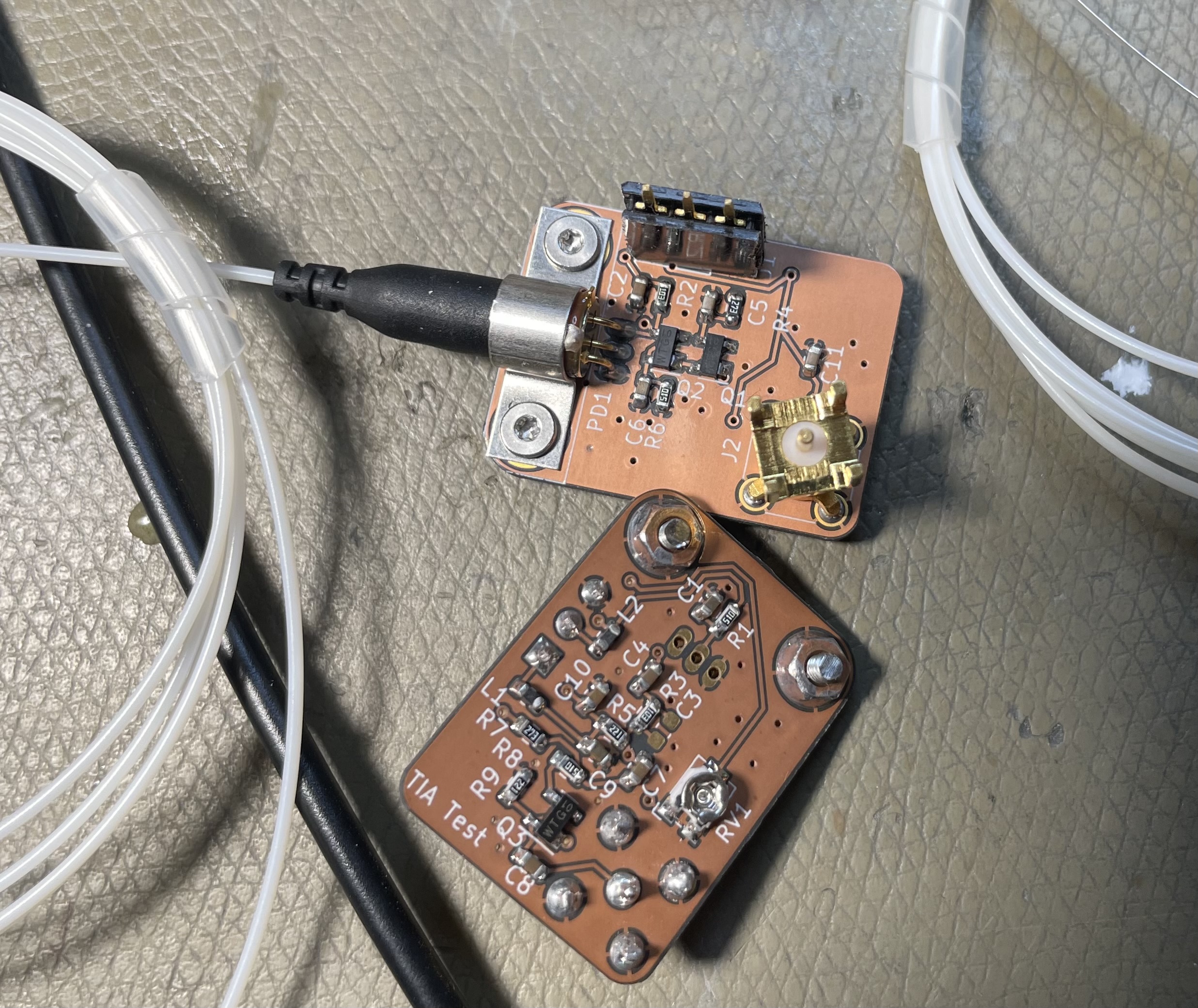
The circuitry is shown below:
Trans-Impedance Amplifier Measurement
The test setup is shown below, an RF generator is applied to the TIA through a high value series resistor. Since the TIA is assumed to operate in closed loop, the voltage at the input base is assumed to be zero. We can then calculate the input current based on the input voltage, and we can measure the output voltage directly.
A DC blocking capacitor and termination resistor is included to ensure that the applied voltage is well defined.

This allows measurement of the current→voltage transfer function, or the trans-impedance gain (V⁄A, or Ω).
For the basic design, a 10 kΩ series resistor was used, since this matches the intended gain of the amplifier core.
Bias current was adjusted using a signal generator for maximum gain and minimal distortion for each test. In general it was found that the bias-level had a major effect on the stability of the amplifier, though it was possible to stabilise in all tested configurations.
Initial Measurement, 220 Ω Collector/10 kΩ Feedback
The initial measurement used the as-designed values from the schematic. Collector resistor of 220 Ω and 10 kΩ feedback.
The applied input voltage was –20 dBm (50 Ω), this corresponds to a voltage of 22 mV RMS into 50 Ω.
The input current then follows as 22 mV ⁄ 10 kΩ = 2.2 µA RMS.
We can then measure the output power vs. frequency. The calculation of gain is simply the output voltage ÷ input current, yielding the TIA gain in Ω.
The TIA gain can usefully be expressed relative to 50 Ω, the gain is calculated as 20·log10(TIA ⁄ 50), and can be compared to MMIC amplifiers.
| Frequency [MHz] | Output Power [dBm/mV RMS] | TIA Gain [kΩ] | Gain [dB] |
| 10 | –26/11 | 5 | 40 |
| 100 | –29/8 | 3.6 | 37 |
| 200 | –34/4.4 | 2 | 32 |
Due to the output buffering and termination, the maximum gain will nominally be half the actual feedback value, so the peak of 5 kΩ is expected. The drop-off at higher frequencies could be equalised in another amplifier stage if required.
Noise measurement involves measurement of the output noise voltage with no RF input, we can then compute the input referred noise floor of the amplifier vs. frequency. The preferred unit for comparison here is A⁄√Hz.
This measurement is performed using a spectrum analyser, and the analyser must be configured such that the output noise floor of the TIA is measurable.
A bandwidth of 1 MHz was used for measurement. The input referred noise floor is then calculated as: noise voltage ⁄ TIA gain = input current; input current ⁄ √BW (1 MHz; = 1000) = noise floor.
| Frequency [MHz] | Noise Power [dBm/µV RMS] | Noise Floor [pA⁄√Hz] |
| 10 | –70/70 | 70 µV ⁄ 5 kΩ ⁄ 1000 = 14 |
| 100 | –70/70 | 19 |
| 200 | –75/39 | 19.5 |
This noise performance is not atrocious, but this is approximately 4⨉ higher than I'd like to see.
1 kΩ Collector/10 kΩ Feedback
The collector resistor was increased to 1 kΩ to improve open-loop gain, tests were repeated.
It was found that the gain and noise floor was flat up to around 30 MHz, and then dropped off at a 1st order rate of 10 dB/octave.
| Frequency [MHz] | Output Power [dBm/mV RMS] | TIA Gain [kΩ] | Gain [dB] |
| 30 | –25/12 | 5.5 | 41 |
| 100 | –36/3.5 | 1.6 | 30 |
| 200 | –47/1 | 450 | 19 |
Noise measurements were performed:
| Frequency [MHz] | Noise Power [dBm/µV RMS] | Noise Floor [pA⁄√Hz] |
| 30 | –75/39 | 39 µV ⁄ 5.5 kΩ ⁄ 1000 = 7 |
| 100 | –82/18 | 11.3 |
| 200 | –90/7 | 15.6 |
The usable gain-bandwidth of the amplifier is clearly reduced. This configuration would be useful for e.g. a HFoF receiver which only needs around 30 MHz bandwidth.
220 Ω Collector/1 kΩ Feedback
This configuration increases TIA bandwidth, but reduces gain as expected.
It was found that the gain was flat up to around 200 MHz, and then dropped off at 10 dB/octave. The 400 MHz drop corresponds approximately to the –6 dB point.
| Frequency [MHz] | Output Power [dBm/mV RMS] | TIA Gain [kΩ] | Gain [dB] |
| 10 | –44/1.4 | 0.630 | 22 |
| 100 | –44/1.4 | 0.630 | 22 |
| 200 | –44/1.4 | 0.630 | 22 |
| 400 | –51/0.63 | 0.28 | 15 |
Noise measurements were performed:
| Frequency [MHz] | Noise Power [dBm/µV RMS] | Noise Floor [pA⁄√Hz] |
| 10 | –88/9 | 9 µV ⁄ 0.63 kΩ ⁄ 1000 = 14.3 |
| 100 | –88/9 | 14.3 |
| 200 | –88/9 | 14.3 |
| 400 | –93/5 | 18 |
This performance is also not fantastic, but is expected.
Summary
The TIA design used here appears to work sufficiently well, but I'm not super amazed by the performance.
The bandwidth as shown below is sufficient for the intended use case:

The major issue in my opinion is the noise floor, which is around 4⨉ more than I'd like to see:

Future work will be to build and characterise a similar design using a S982 dual-gate MMIC amplifier. This could potentially improve on the noise performance, and in principle may have sufficient bandwidth for the job in most cases.
The downside is that this IC is obsolete, so others will have trouble reproducing the design.
Here's a sneak preview of this circuit:
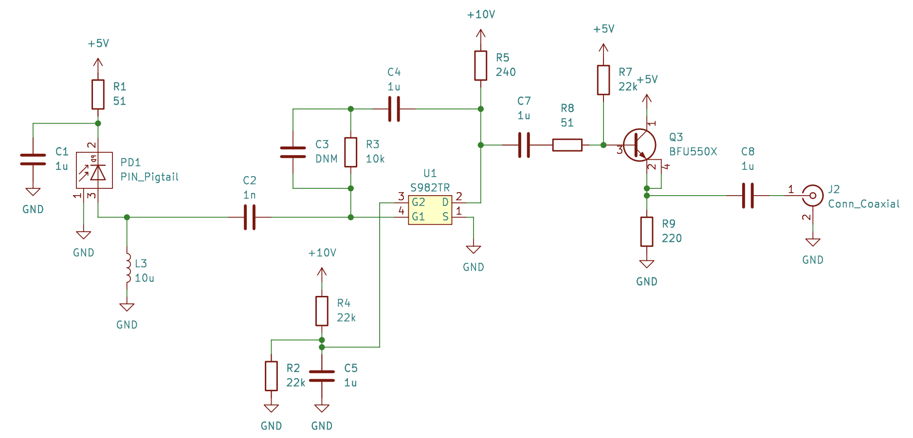
This version is intended to be optimised for higher bandwidth, so an inductor is used to ground, though it could be replaced by a resistor as well.