A Smart C-MAC STP 2373LF OCXO

The C-MAC STP 2373LF is a 2⨉2⨉1" OCXO used in e.g. the Epsilon EC2S GPS clocks. Since a number of these clocks were broken in obvious or subtle ways, I decided to reuse the OCXO's and other useful components from these.
Table of Contents
The Concept
My idea for reusing these OCXO's was to use them as the master timebase for e.g. a new GPSDO using a more modern receiver, like perhaps the Furuno GT-88, or even a long-wave radio clock such as TDF162, BBC 4 AMDSS, or even DCF77 receiver.
I wanted to implement this OCXO as a separate subsystem in order to skip having to re-implement all the required OCXO control hardware and software for each project. This essentially means making a smart OCXO.
The desired feature set included among others:
- Built in high resolution DAC
- Tuning voltage storage
- OCXO parameter storage (informational, tuning sensitivity, drift parameters)
- Built in test & monitoring
- "Normalized interface" - allowing multiple OCXO types to be used with the same clock hardware
At the time of writing I haven't performed any proper integration of the OCXO into a system yet. However, after an initial tuning the OCXO seems to be extremely stable, and seems to stay well within the 1⁄100th to 1⁄1000th Hz range relative to my GPSDO's. This is even the case after multiple power cycles with no re-tuning.
This extreme stability is highly desirable, since it can allow extremely slow PLL time constants when disciplining, improving the often mediocre short and medium term stability of both radio and GNSS clocks (and especially atomic clocks).
Implementation
Because I felt like it, I decided that implementing this design as a fairly large (and expensive 😢) flex-PCB was the right solution.
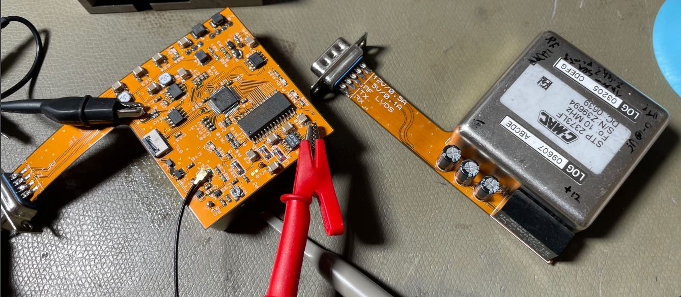
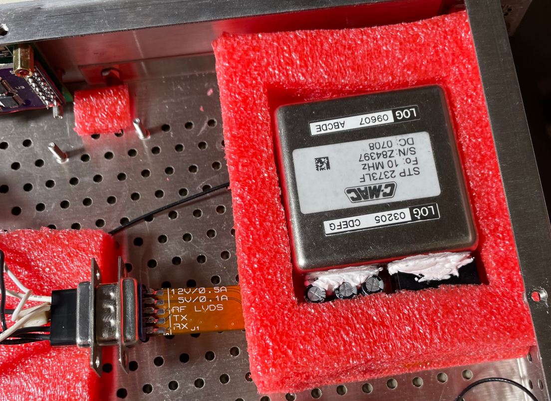
The flex PCB consists of a large rectangle soldered to the OCXO, containing all the circuitry, and a flex-arm soldered to a standard 9 pin D-Sub connector for the interface. This means the OCXO can easily be put inside a foam insulator with the arm poking out.
The OCXO
I don't have a datasheet for the OCXO, but C-MAC OCXO's seem to be highly regarded in the time-nuts scene. The performance achieved thus far is quite good.
The pinout is standard, the middle pin seems to be a voltage reference output, with around 6.7 V on it. I didn't use this output in my design since the DAC has a built in reference.
The heater power seems to peak at around 6 W at 12 V, and settling to 2 W without additional insulation. With a foam box around it I have seen powers approaching 1 W.
The output is a fairly strong 10 MHz sine wave.
The pinout and package seems to be equivalent to a Morion MV267, though the C-MAC is around 19 mm tall.
The Processor
The processor for this system is a STM32F103C8T6; this is a somewhat excessive choice, and I mainly selected it due to requiring a large number of I/O pins for the DAC. Otherwise a STM32F0 would be more appropriate. I would also like to get rid of my supply of these MCU's since they're quite lacking in features compared to newer devices in the series.
The processor implements the control software, and communicates over serial. There is a 16 kbit F-RAM chip suitable for local storage of various parameters. All data is stored double buffered with checksums, as expected.
Power System
The power system is a split design, with an external 12 V driving the oven directly, and generating a ±15 V supply for the tuning system. There is a separate logic power supply, which is nominally 5 V, though up to 20 V can be applied without damage.
I included measurement of the OCXO current and the external 12 V to allow OCXO power to be calculated.
Tuning DAC
The tuning DAC is one of the most important devices in an OCXO design, the performance of this + the voltage reference can easily be the limiting performance factor.
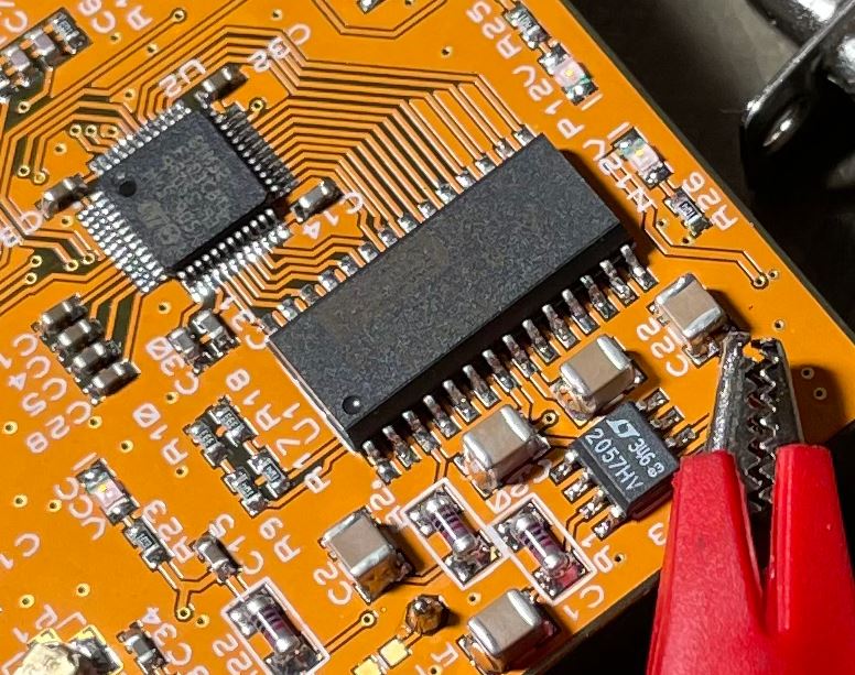
For this design, the DAC715U was selected as the DAC, mainly since that's what the Epsilon clock used already, so I could just unsolder it from those clocks and reuse it here. This DAC is a 16 bit parallel load type with a 0-10 V output voltage range (internal reference).
This DAC annoyingly demands a ±12-15V supply voltage, hence the need for a DC/DC converter on the board. (In the Epsilon clock this was generated using a 7660 type charge pump).
The DAC output is filtered in two 1st order RC filters (8 Hz cutoff), then buffered in a LTC2057 chopper opamp, and applied to the OCXO tuning pin through another RC filter (to attenuate the opamp's clock feedthrough). High stability SMM 0207 thin film MELS resistors were used for these filters, though this is mostly a flex.
This DAC can be updated quite quickly, and the software implements 64x oversampling, giving an additional 6 bits of tuning resolution, making the total system capable of (in theory) 22 bits resolution.
Software
The MCU software is standard stuff, STM32 HAL with a couple of state machines, UART DMA's, ADC readout routines, etc.. The software performs a variety of internal self tests on startup, keeps track of power-on time (current and cumulative), and allows the setting and reading of the DAC tuning word.
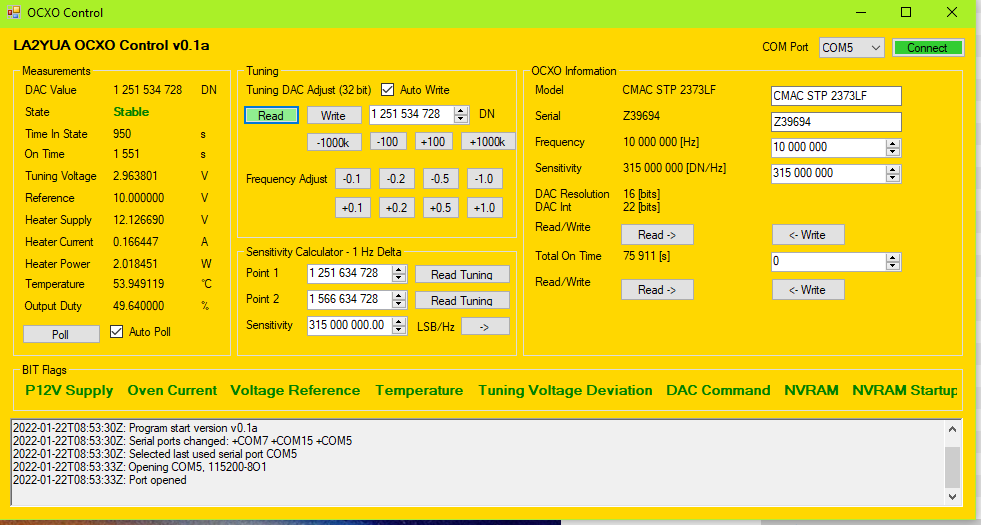
There are a variety of self test features, though the only self test that actually matters is a tuning DAC failure. This is since almost any failure can be tolerated as long as the OCXO can tune itself. To ensure this is the case, there is a readback of the DAC output to the MCU's ADC. This performs a 3-point check of the DAC at middle, maximum, and minimum tuning voltages on startup.
As seen in the PC control software above, there are several other BIT flags that can be set depending on mode, and checks are made of the 12 V supply, oven current (mode dependent), temperature, tuning voltage, and NVRAM errors.
The software also implements a warmup delay on startup, which is currently set to 10 minutes. The OCXO seems to warm up to very good stability within 10 minutes or so. There is a check for the loss of external 12 V, which triggers a new warmup wait if detected for more than around 30 seconds.
As seen above, a 32 bit tuning word is used for the external interface, and the OCXO reports the actual hardware DAC and interpolated DAC resolution. This 32 bit interface is considered to be sufficiently high resolution for any normal use case, and it's trivial to shift this down to whatever resolution is required in the OCXO. The OCXO also reports its tuning sensitivity in DAC LSB⁄Hz, i.e. what change to the 32 bit tuning word causes a 1 Hz frequency change.
I included a calculator in the PC software that can read the tuning voltage at two points and tell you the difference, so to determine this factor I first the OCXO dead on 10 MHz, store the tuning word, then step it manually to get a 1 Hz offset and store that word as well.
This information will be used as part of the calculation of PID regulator gains when controlling the OCXO - in theory an OCXO with different gain factors can be swapped in later without retuning when this factor is accounted for.
For the specific unit shown above, this is corresponds to around 700 mV per Hz at 10 MHz, or around 330'000 LSB's in the 22 bit domain (in theory giving a 3 µHz tuning resolution).
Dithering
The DAC interpolation is performed using basic dithering.
A 32 bit input value is input, this is then shifted down to 22 bit, and a sawtooth ramp of length 64 (the oversampling factor) and amplitude 64 is summed with this value, before shifting down to the 16 bit DAC resolution. This generates a 64 long array of 16 bit values containing a square wave with an amplitude of 1⨉16 bit LSB, where the duty cycle corresponds to the sub-LSB value. If the median over the array is taken, the average should be close to or equal to the 22 bit value we started with.
That is, if we just output these values to the DAC and low pass filter the output, we will get a value in between what the two 16 bit values would give.
An annoyance with this method of generating the oversampled data is that the data represents a square wave at the lowest frequency possible given the oversampling ratio (period = oversampling ratio). In order to increase the high frequency content, noise shaping methods could be used.
I simply chose to read out the data in an interleaved fashion, i.e. first outputting element 0, then element 32, 1, 33, etc.
The DAC is parallel, and access time is an issue. Especially since the wiring of the DAC was selected for routing simplicity. This means that each bit of the DAC data must be re-mapped to some specific pin (on an arbitrary I/O bank), which is relatively slow.
In this system, the update time is crucial, not the time to generate the 64x oversampled data. As such, I generate a 64 bit array of length 64, and pre-calculate the GPIO bank's BSRR (bit set-reset register) for the two GPIO banks the DAC pins span. This register is a 32 bit register where the lower half is what bits to set on that I/O bank, and the upper is what bits to reset.
This allows atomic set & reset operations on the register without needing to do a read-modify-write cycle. By pre-calculating what I/O pins are set and reset for each step in the 64x oversampling, an ISR can simply iterate across this array and write the BSRR values to the GPIO banks + pulse the DAC latch pin. This cut the DAC access time down from ~50-100 µs to less than 1 µs, making this fairly high oversampling ratio practical.
Potential Issues
The biggest issue with this design is that the OCXO control hardware operates at fairly extreme temperatures, typically 70-80 °C when installed in a foam box. This may be a long term reliability issue, though performance thus far seems acceptable.
I fully expect the electrolytic decoupling capacitors to degrade within a few years, but these are not essential for the functionality of the device.
This elevated and stable temperature is a benefit for e.g. DAC and reference stability, since these basically have no thermal drift.
The NVRAM (F-RAM) has relatively poor data retention times at these temperatures, but this is solved by re-writing the F-RAM (double buffered) every 5 seconds.