HF over Fiber — an optical Mini-Whip antenna
In this article I'll briefly talk about my newest Mini-Whip antenna project, designed primarily to cover the lower bands.
Table of Contents
The Problem
My existing Mini-Whip implementation has a few issues that I wanted to correct in my new design. These issues include:
- Lack of front end low pass filtering causing desensing and intermodulation when VHF+ transmitters are active
- Slightly higher than needed input capacitance due to lazy design
- Ground loops causing mode conversion and HF noise
- Distribution to multiple devices is problematic because of ground loops, especially when computers are involved
- I want to distribute the signal to:
- ITT Mackay 3021N HF receiver
- AirSpy HF+
- DCF77 time decoder
- Spectrum Analyzer
- Others as needed, both permanent and temporary
To resolve these issues I did some design work on the basic mini-whip design, and I decided to use fiber optic transmission (RF over Fiber) for the RF output since I had a bunch of suitable fiber coupled laser diodes sitting around.
The principle of RoF is to amplitude modulate light that is transmitted in a fiber optic cable, the amplitude modulated light can then be "rectified" using a PIN photodiode or similar device (APD's can also be used).
Since the modulated light has a wavelength of e.g. 1550 nm, the "carrier frequency" is approximately 193'414'489 MHz (or around 200 THz). This means that the RF bandwidth you can modulate onto this carrier can be quite wide. The practical benefit is that the length-bandwidth product of coaxial cable no longer applies, and fiber optic splitter are basically perfect devices so distribution of a fiber optic signal is very simple.

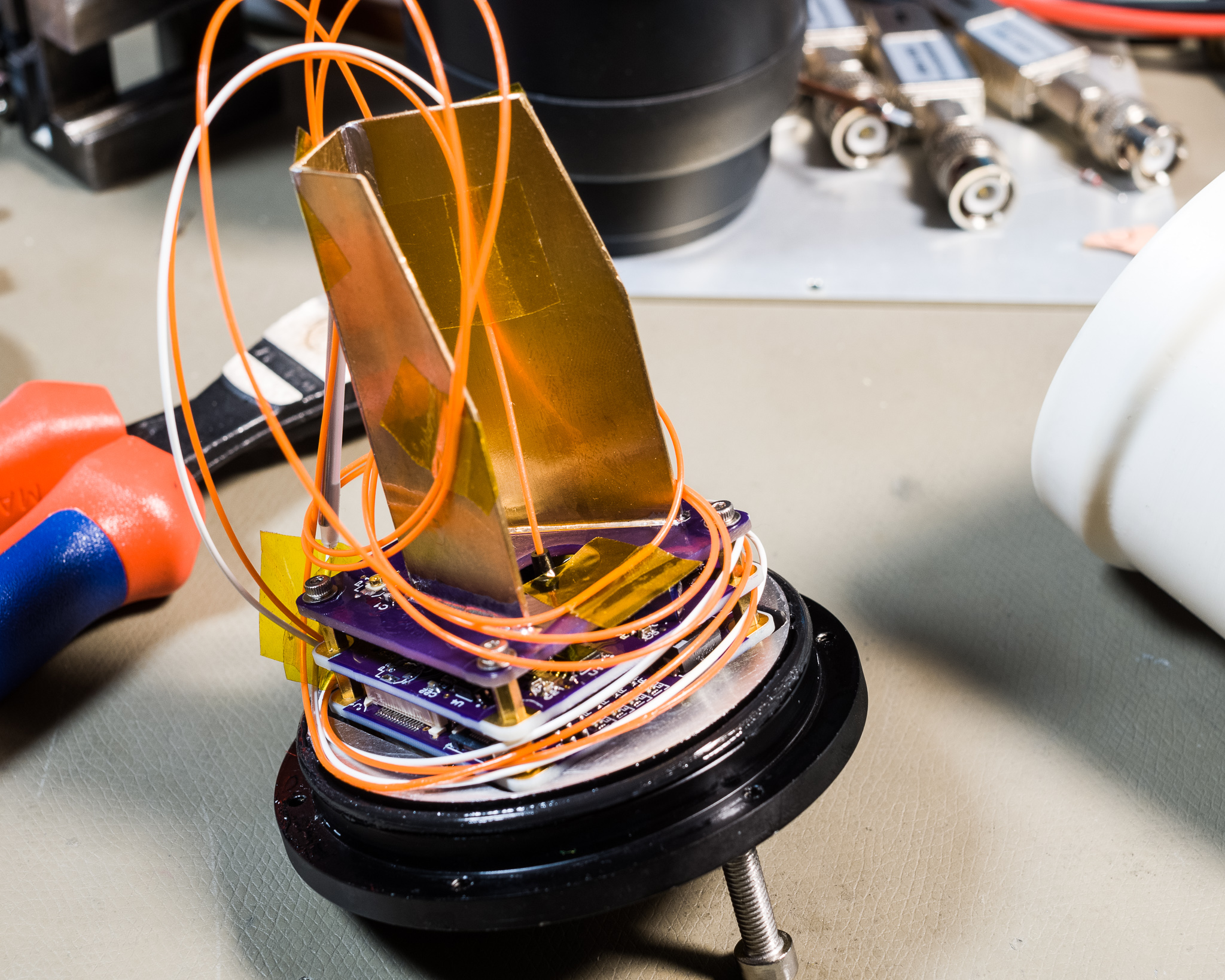
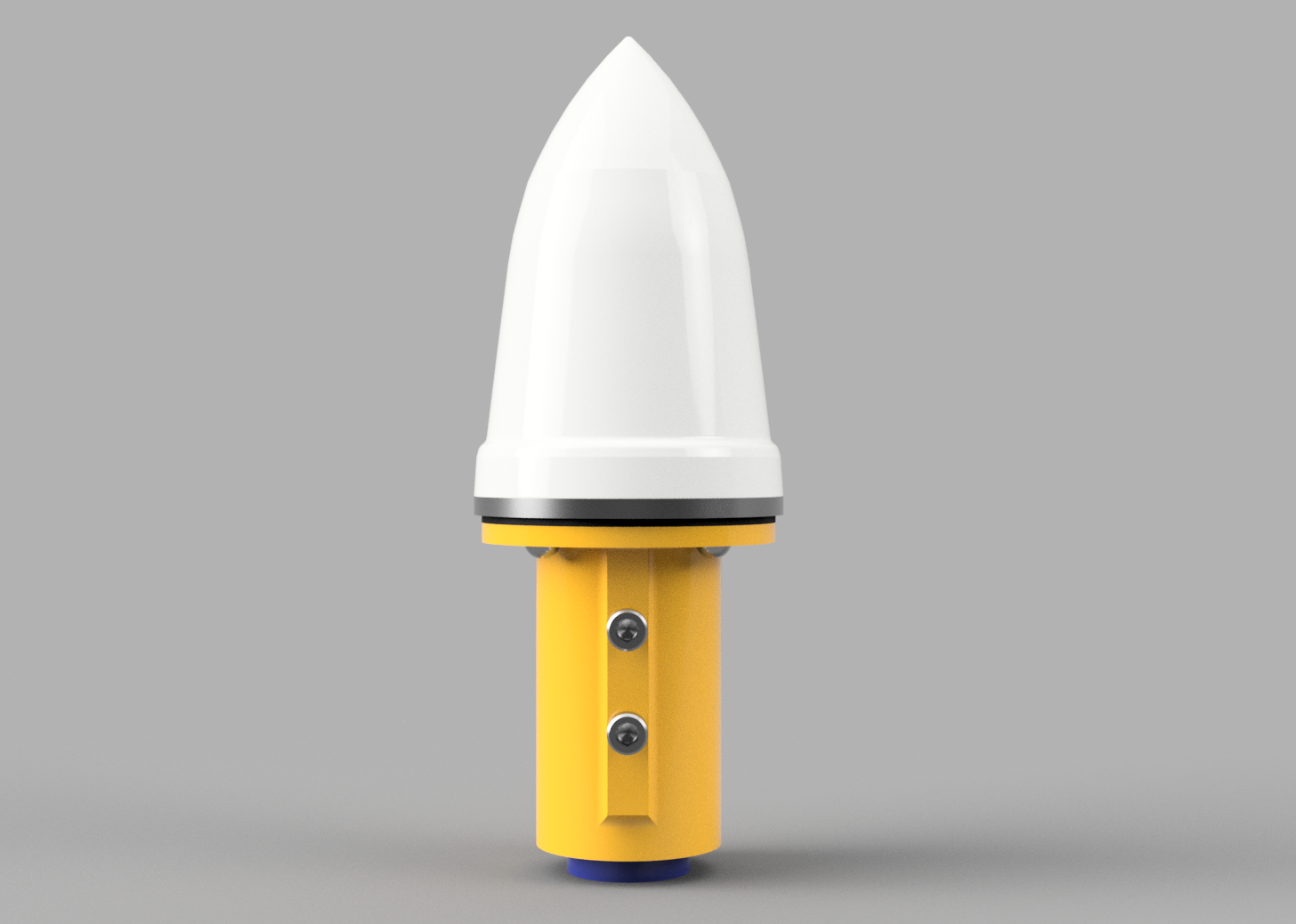
The final implementation uses the housing from a PCtel GPS antenna that can be bought quite cheaply from China, and a custom 4-board vertical stack of electronics.
Mini-Whip Amplifier Design
As should be well established, a Mini-Whip is the name of a specific type of broad band E-field antenna. The basic principle is to use a very high input impedance voltage amplifier with a relatively small electrode to pick up the signal.
The principle is quite similar to leaving a 1 MΩ input oscilloscope input floating.
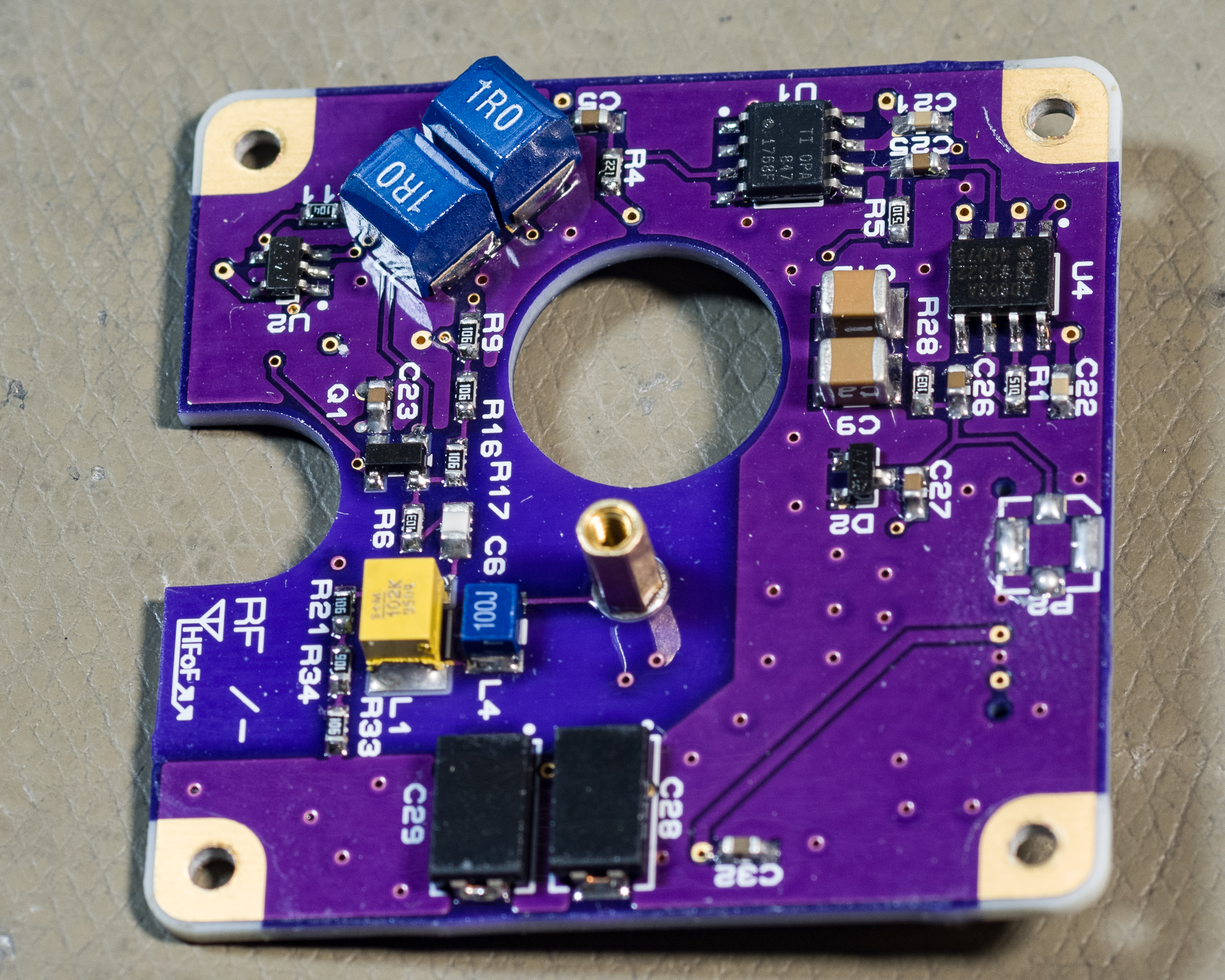
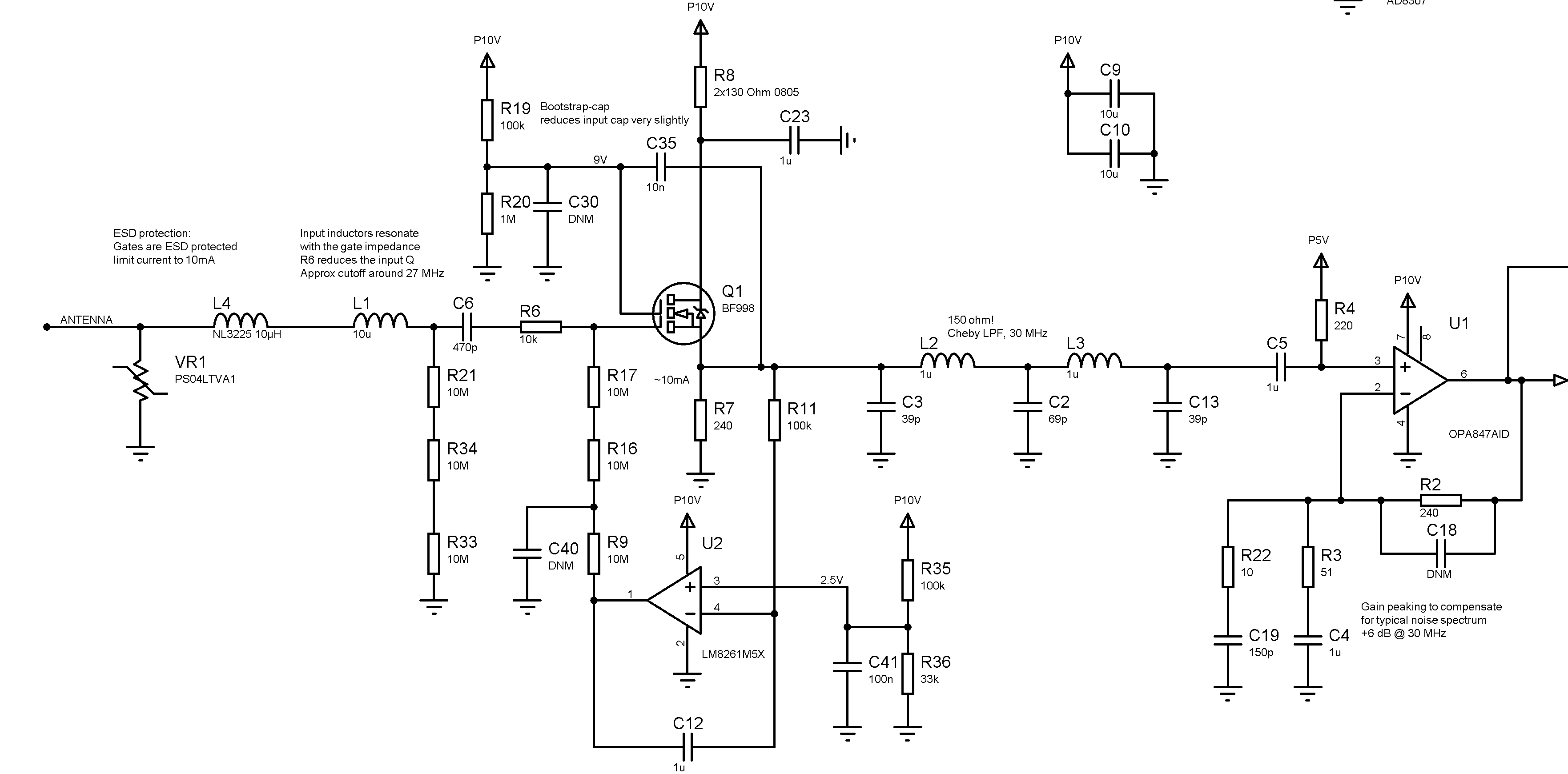
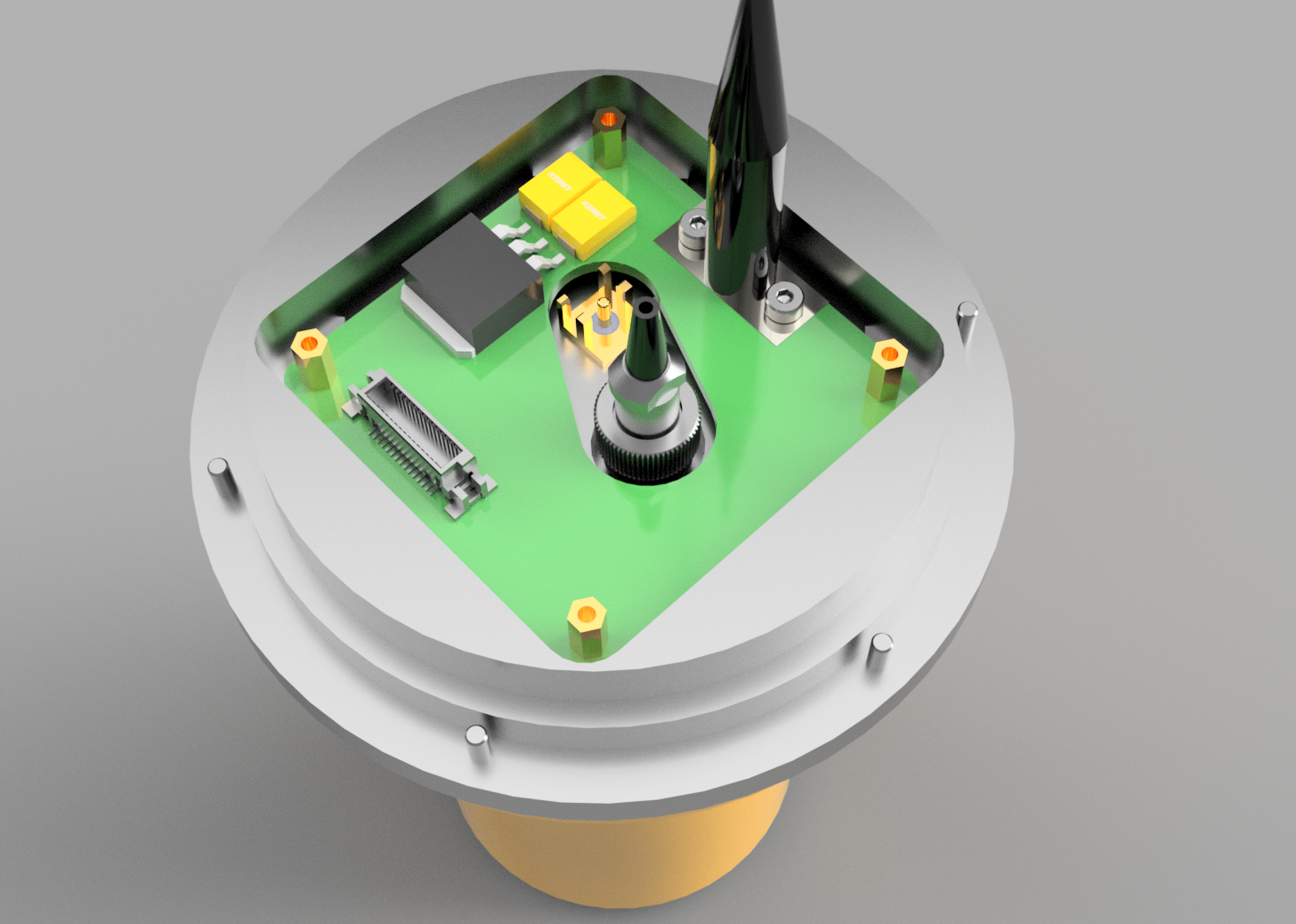
Above the finished PCA is shown, as well as the "Mini-Whip" part of the schematics. The antenna electrode is connected via the soldered in M2 brass spacer.
A low capacitance varistor is used for ESD protection of the input. The primary function of the input is to act as an impedance converter, or a buffer amplifier. The goal is not to provide voltage gain, but rather to provide the absolute minimum input current noise density and capacitance. A BF998 was chosen for this application since it was available, and has better capacitance specifications than the typical U310 JFET.
The FET circuitry is actively biased to operate at around 10 mA using an opamp integrator. Note also C35, this bootstraps the Gate 2 input, providing a very slight reduction in input capacitance vs. installing C30.
The input filtering is accomplished with two 10 µH inductors, giving a cutoff around 27 MHz. These inductors resonate with the gate capacitance, and R6 is a 10 kΩ resistor added both to limit gate current and reduce the circuit Q. Effectively we then have a RLC low pass filter.
After the impedance converter, the output is considered to be 200 Ω nominal impedance, and a low pass filter configured for 30 MHz is inserted to further reduce high frequency interference. An OPA847 wideband opamp is used as a voltage amplifier with a slight gain boost at higher frequencies.
At the output of the OPA847 is both an AD603 IF VGA, and an AD8307 power detector. These are used to implement AGC to optimize the drive level for the laser diode.
The final RF output from the VGA is routed through a board-to-board stacking connector, ending up at the laser diode in the base PCA.
Control Section
The fiber optic aspect of the design requires active power control of the laser diode, and the laser diode link has linearity issues that necessitate the use of RF automatic gain control.
To control these features, the control section uses a STM32F030 microcontroller to read the various control signals such as temperature, current, RF level etc. and control the laser diode bias circuit, and the AD603 VGA amplifier.
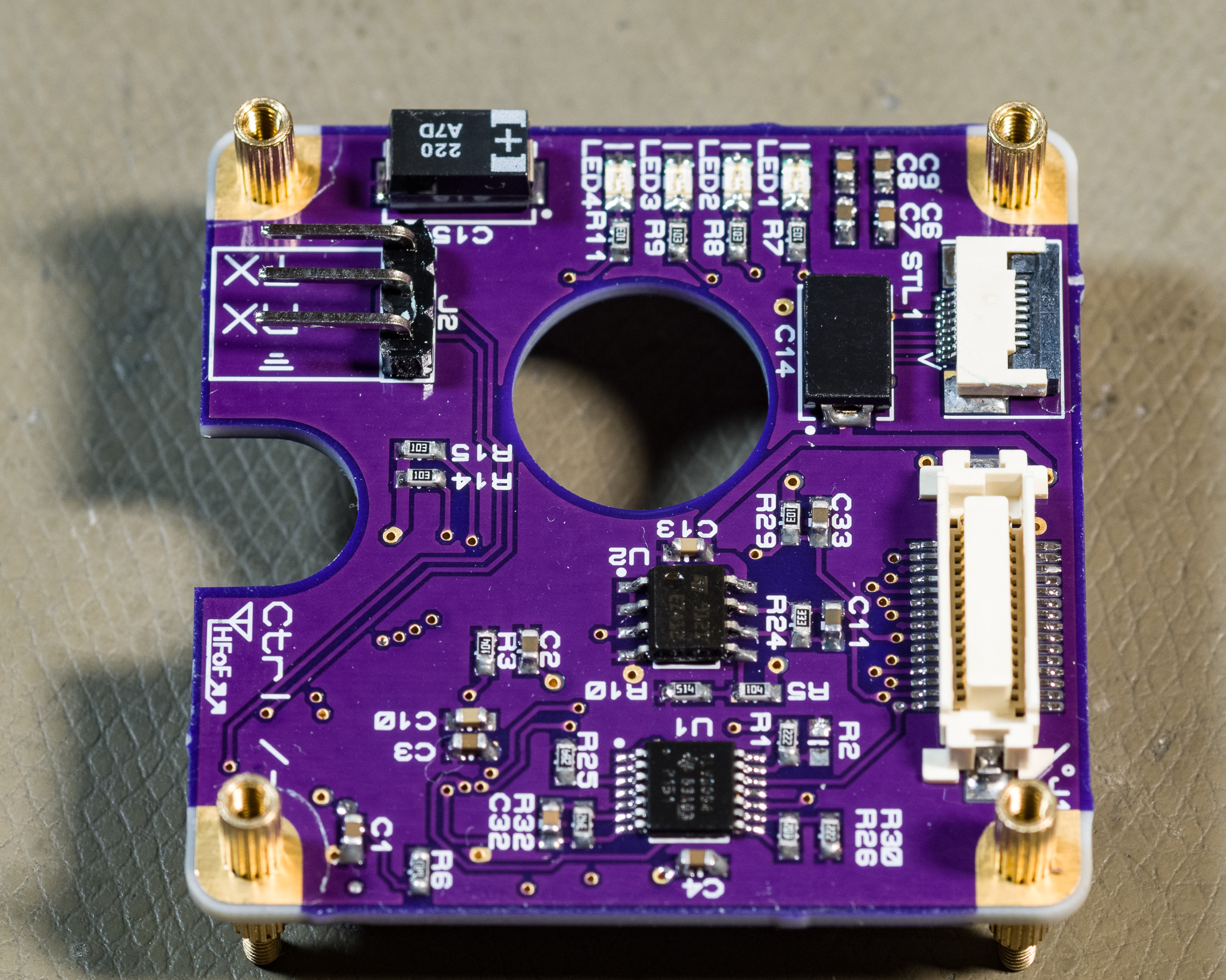
The MCU is located on the bottom layer, and some attention was paid to optimizing the layout of the PWM DAC outputs for EMI.
A TTL level UART port is used to remote control the device during calibration. A I²C EEPROM is also present to store calibration values. A C# program was written in a hurry to monitor and calibrate the device.
Power PCA
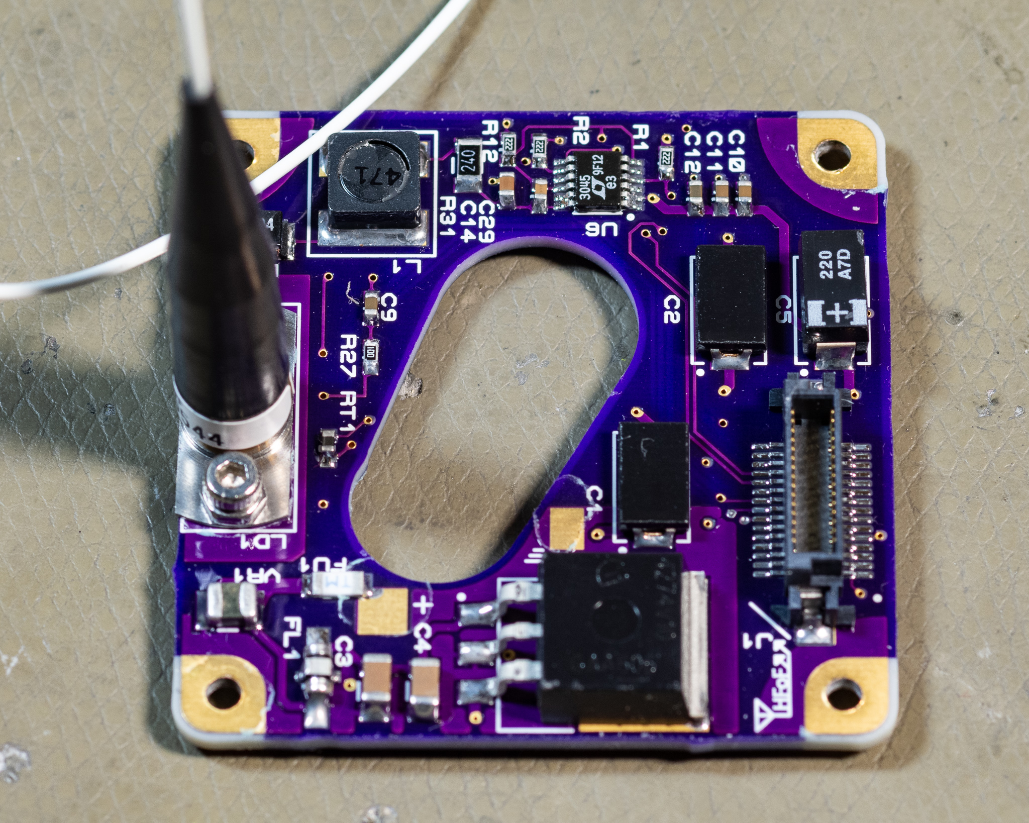
The Power PCA sits in the bottom of the stack, and contains all the primary heat generating components. In system a large thermal pad sits between the PCA and the antenna base.
The power input is nominal 14 V, with a withstand rating of 24 V and design goal of no catastrophic failures at 48 V. The input is via a bottom mounted SMA connector, this is wired to pads on the PCA, providing some degree of strain relief.
A TLE4274 linear regulator is the primary input regulator, this generates 10V and is designed for automotive applications. Because of this, it is capable of withstanding ±48 V without further components. At the bottom of the board, there are linear 5 V and 3.3 V regulators.
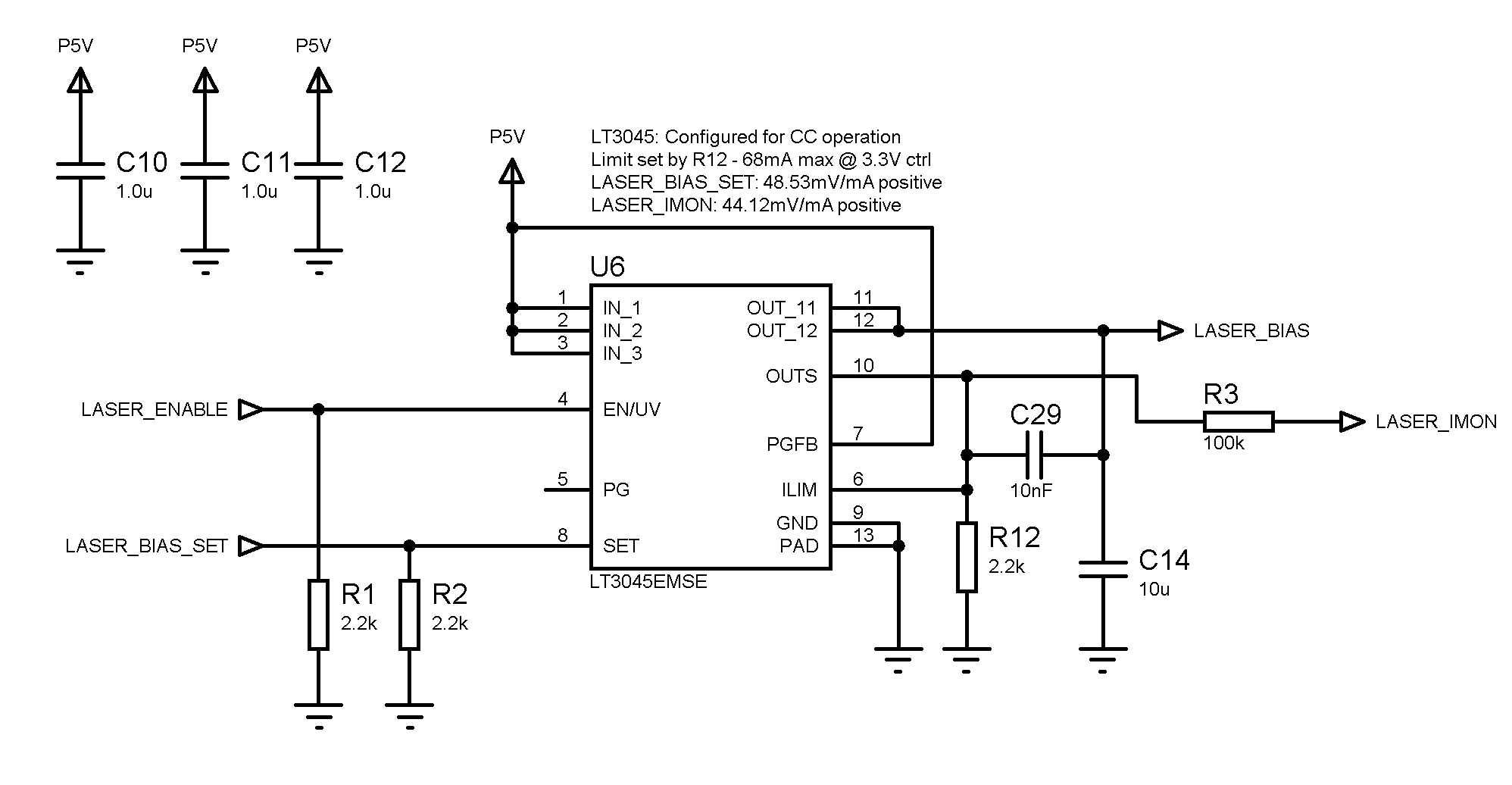
The laser diode bias generator is based on a LT3045 linear regulator. This device is probably more sophisticated than required, but it has the advantage of being fully protected against thermal issues, which a discrete solution normally won't be. The device is normally a voltage regulator, but by using the ILIM output for the voltage feedback the device will operate quite happily as a constant current source.
The MCU can then set the output current using a precision ground referenced voltage, and the ILIM port can also be measured to verify that constant current was achieved.
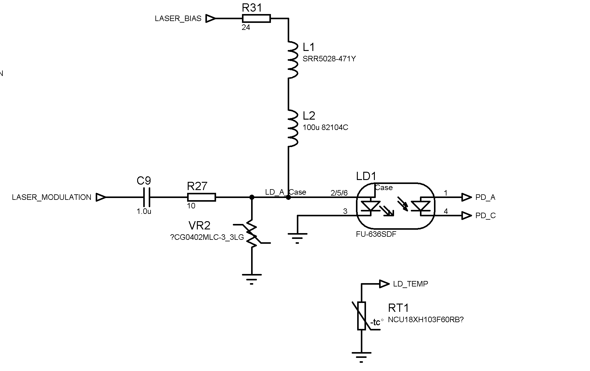
The laser diode is a Mitsubishi FU-636SDF, 1550 nm and around 2 mW. This diode also includes a monitor-photodiode that is measured by the MCU. An external thermistor is used to temperature compensate the target output current, and as a protection feature.
The diode connections are very similar to an RF amplifier, where a bias-tee is used to provide DC current, and the modulation is AC coupled in. Annoyingly the case of the diode is also the anode, so the entire case presents a somewhat large load, but this isn't an issue for HF operation.
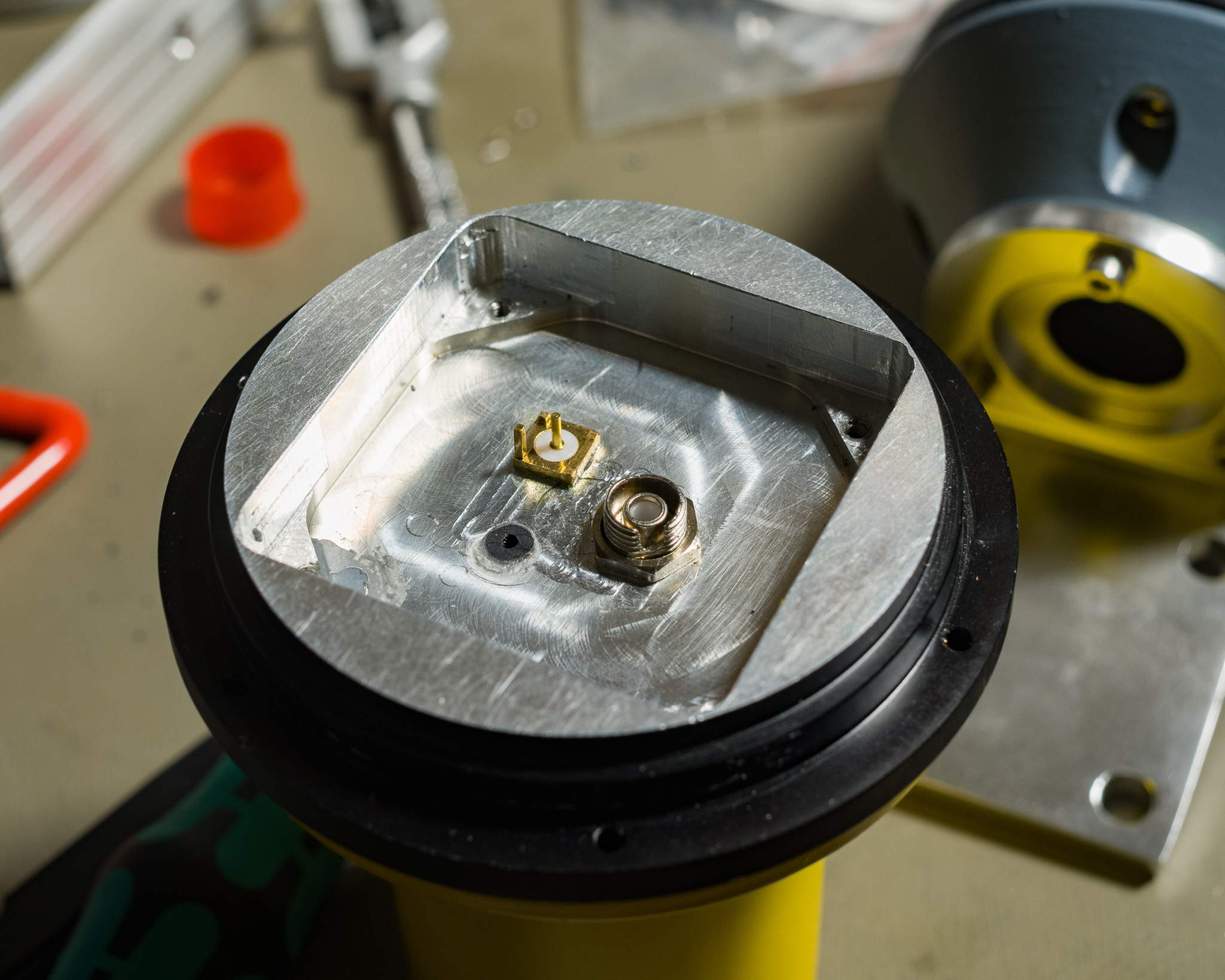
A vertical orientation was the only possible orientation that would maintain reasonable fiber bend radii. The diode is screwed down to the board using soldered M2 brass nuts, and the leads are soldered to pads on the bottom layer.
Assembly
The assembly is relatively simple but tedious, each board is installed using male-female brass spacers in series. The fiber optic output is via a FC connector, and the output connector must be pulled through all the boards and installed before the boards can go in.
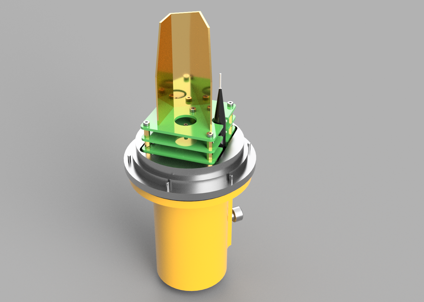
At the top is the antenna board, a 2 layer PCB with a ground plane on the bottom layer. This is not good for the input capacitance, but I considered it necessary to prevent RF feedback to the antenna. The antenna element for the first two devices is made from 1 mm thick brass plate, this gives a very nice feeling antenna. In practice the antenna would likely work just as well if I had made the antenna panels from copper clad circuit board.
The antenna PCA also includes a UFL connector with a 2 pF series capacitor, this means a normal 50 ohm source can easily be connected to the amplifier to verify performance.
The laser is a pigtail type, and I spliced on a standard FC/UPC connector pigtail. The length is a bit excessive, at around 2 meters of spare fiber.
2021 update: I have since determined that analog RF systems should always use APC connectors to avoid laser oscillations caused by reflections. This effect was not a major issue with this specific design, but did cause several other issues with later designs using higher frequencies.
Mechanicals
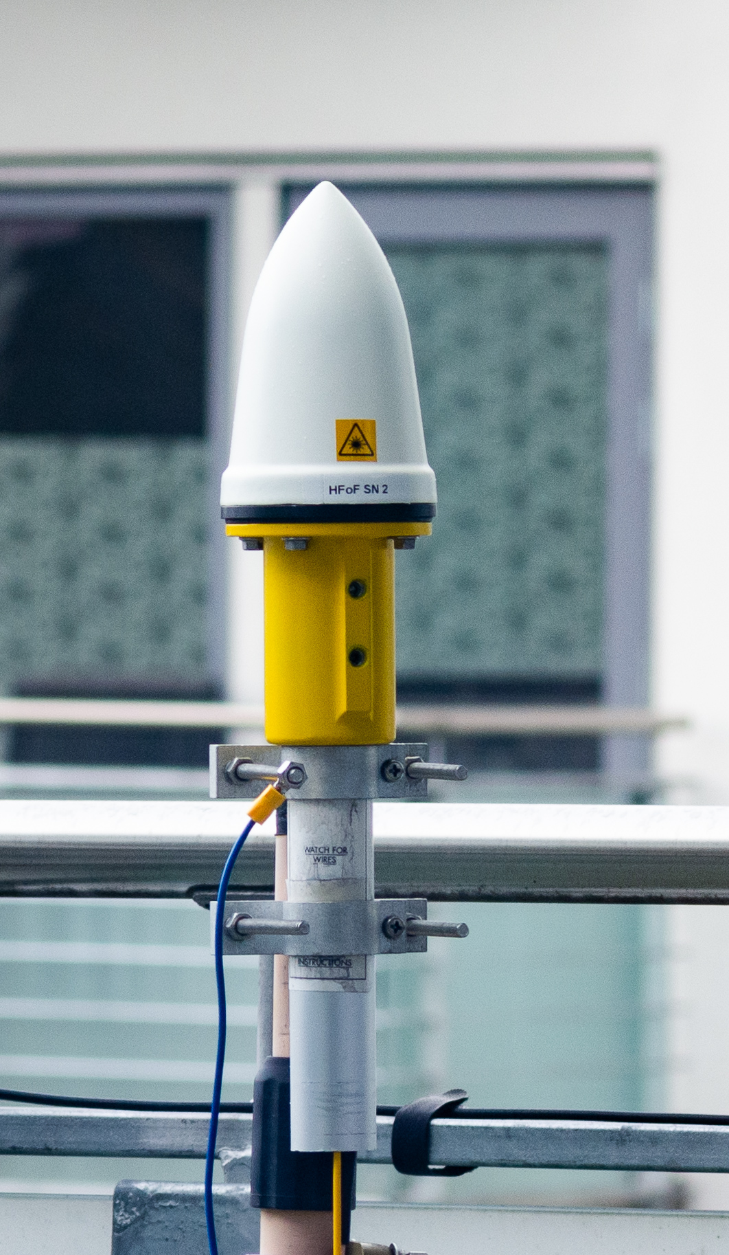
The antenna is built in the chassis of a PCtel GPS timing antenna, this antenna is very cheap to buy used if you don't mind making your own non-standard mounts.
I happened to have one mount available, since I bought a new-in-box unit back in 2016.
The base part of the antenna was machined to plug the hole where the original N connector sat, and the height of the bottom PCB was lowered to 2mm above the base to improve thermals and free up space for the antenna element.
The entire assembly (minus the fiber optic wiring) was modelled in Fusion 360 before designing any PCBs. This significantly reduced the risk associated with the design, since all critical mechanical dimensions and alignments could be verified before design and construction.
Below are some renders made before anything was built:
Over all this way of working was a huge success, board-to-board connectors are a particular place where mistakes are often made. The only mechanical issue I had with this assembly was slightly too small mounting holes on the boards, but this was easily solved with a drill.
Performance
The antenna as installed works quite well, providing strong reception down to 16.3 kHz and lower (16.3 kHz is a NATO submarine transmitter). LW and MW performance is excellent, exceeding my previous antennas performance wrt. random noise in A/B testing. HF performance seems reasonable, but conditions have been poor lately.
The limited dynamic range of the laser diode is not an issue for my setup since my local noise floor is high enough that the effective dynamic range is quite low.
A very slight gain reduction is seen when 25 W 145 MHz FM transmissions are sent, this seems to be caused by coupling into the power detector and no interference is visible in the HF spectrum.
Distribution
The system implementation around this antenna is quite similar to - and uses some common components with — a fiber optic analog cable TV system.
These systems typically modulate a specific wavelength with RF (1550 nm; sometimes around 1650 nm is used), covering around 45-860 MHz. This can be distributed over large distances and converted to electric as needed with effectively no length dependent loss or bandwidth reduction.
The basic method of distribution is via optical splitter, and my system currently uses a 1:8 splitter. This obviously attenuates the signal, but starting around 1-2 mW the losses are quite acceptable. Adding an additional splitter in line will likely require active detectors to work.
To convert the signal back to RF at each end-point, fiber coupled PIN diodes are used. This sounds expensive — and normally would be — but it seems that the Chinese market likes the CATV over fiber concept described above, and passive FTTH detectors can be bought for very low cost off sites like AliExpress.
These detectors contain a InGaAs PIN diode glued into a SC optical connector, and in the original case a parallel inductor is used to operate the diode in "solar panel" mode. All the RF is generated by the diode. Replacing the inductor with a resistor in the 50-250 Ω range and increasing the capacitance at the output will easily convert these detectors to a VLF capable detector. There is some minor loss of sensitivity at higher frequencies after the mod, but this is fairly insignificant.
The AGC in the antenna has been set such that with the splitter losses and the efficiency of the passive detector, no significant reduction in noise figure occurs, but the signal levels are very low and receivers expecting amplified antennas can have issues because of this.
Below are two types of detector using this principle that I got off AliExpress seller DN Optical Communication Store (no relation/sponsorship, good products though).
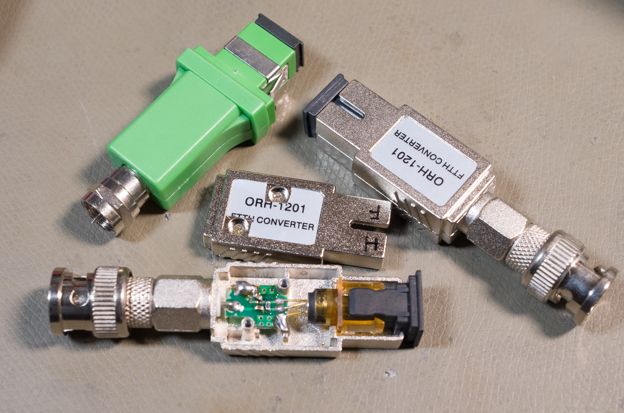
Note that the metal covered ones also have an F connector, the BNC adapter was bought separately. There is no real quality difference between the two types, both seem to use the same diode and use the same circuitry, obviously the metal shielding is a slight benefit and gives a premium feel. Cost is typically well below $10 per unit, depending on the quantity.
The green type above is superglued together and quite hard to open. There is also an orange plastic type available that is easier to open and assemble again.
The plastic types are generally easier to re-use for other purposes, such as this experimental transimpedance amplifier for HF operation:
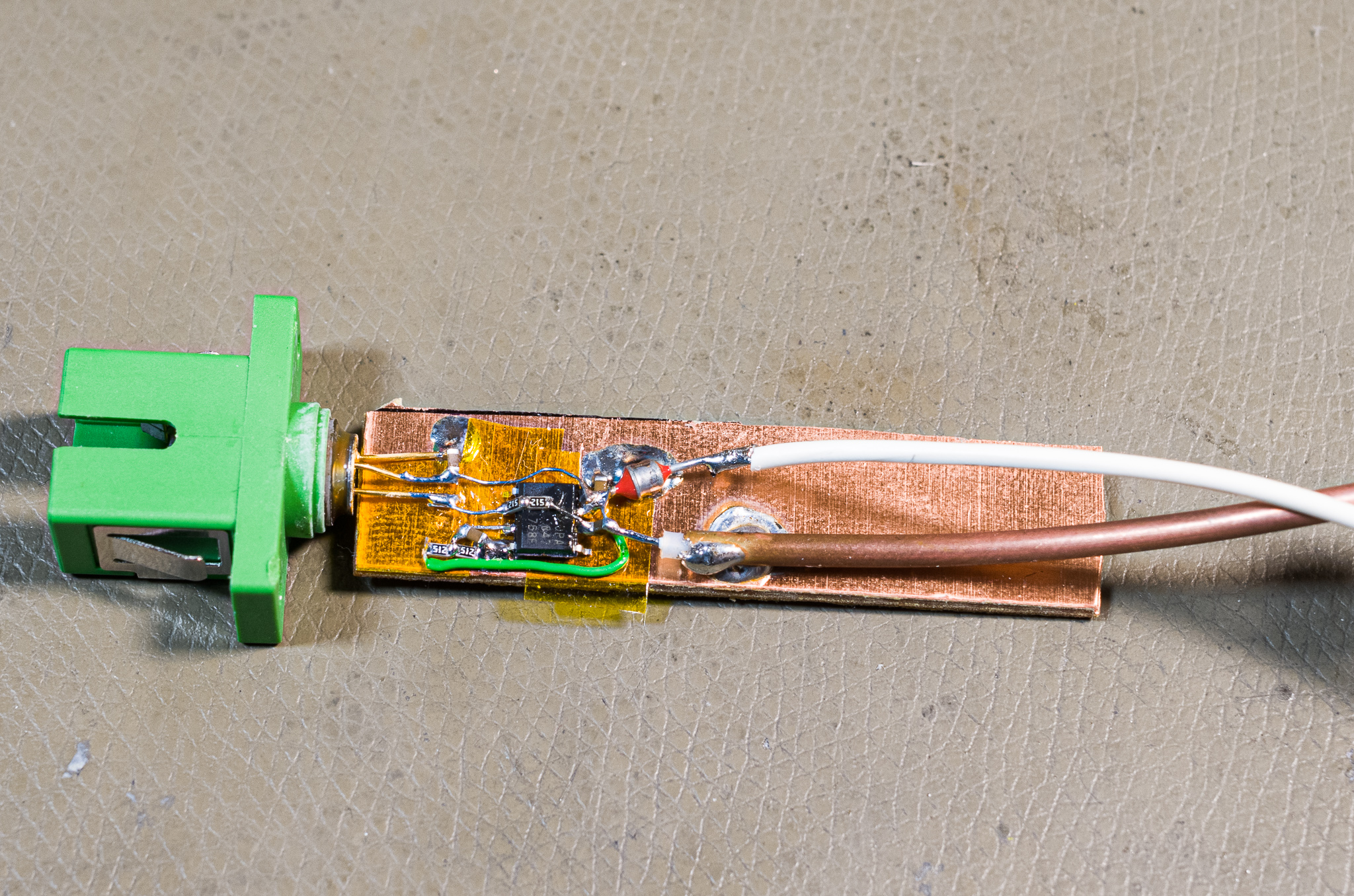
The above amplifier is the alternate way to detect the signal, and using an active low noise transimpedance amplifier is a better way of detecting the signal if losses are significant. These amplifiers can also be tuned for the specific frequency band in use, but they require power to operate.
I expect to primarily use this concept for receivers that expect a specific frequency range and already expect powered antennas. An example is the DCF77 receiver, that outputs 5 V on the coax and expects a fairly strong signal because of it. A basic amplifier that operates off 5 V bias with 22 kΩ gain (~500 kHz BW) has been prototyped inside one of the metal cased detectors for this purpose.
Future Plans
My future plans for the project include building a VHF/UHF (50-500 MHz) variant of the same antenna to provide essentially full coverage for general purpose receive only applications. I expect to modify all the PCAs somewhat, since the amplifiers and some implementation details will be different for the higher frequency coverage. Especially the AGC system will have to be different.
I may modify e.g. my 3021N receiver and other devices to accept fiber optic directly, with the TIA installed inside the device.
In addition, making some active distribution amplifiers for e.g. in-rack distribution seems like a good candidate. For HF this will likely use a OPA847 as a discrete transimpedance amplifier.
For the VHF/UHF variant the Maxim Integrated MAX3654 "47MHz to 870MHz Analog CATV Transimpedance Amplifier" IC seems like a very good amplifier for the job. Unlike most amplifiers this has a very wide bandwidth and is designed for analog operation (most TIA ICs are designed either for LIDAR application with lower bandwidth, or for digital systems).