The 3021N OCXO Card (Part 10)

The OCXO card is a somewhat standalone reference oscillator made for the 3021N receiver. This card was finished in late 2022.
Note that this part of the series is published out of order, at the time of first issue this PCA has not been integrated into the radio, but a copy of the PCA has been integrated into a 19" rack unit.
Table of Contents
Design Description
The OCXO card does not replace any existing assembly in the radio, and it's more or less an optional add-on (though removing it requires some frame wiring changes to re-route the external reference).
It is basically a primary timebase in the system, in charge of keeping the tuned frequency of the radio highly stable even if the external 10 MHz is removed.

The card is intended for continuous operation, and generates a 10 MHz square wave output at all times unless a major BIT failure occurs. It is connected to the Synth external 10 MHz input, and disciplines the VCTCXO that is actually used for the radio.
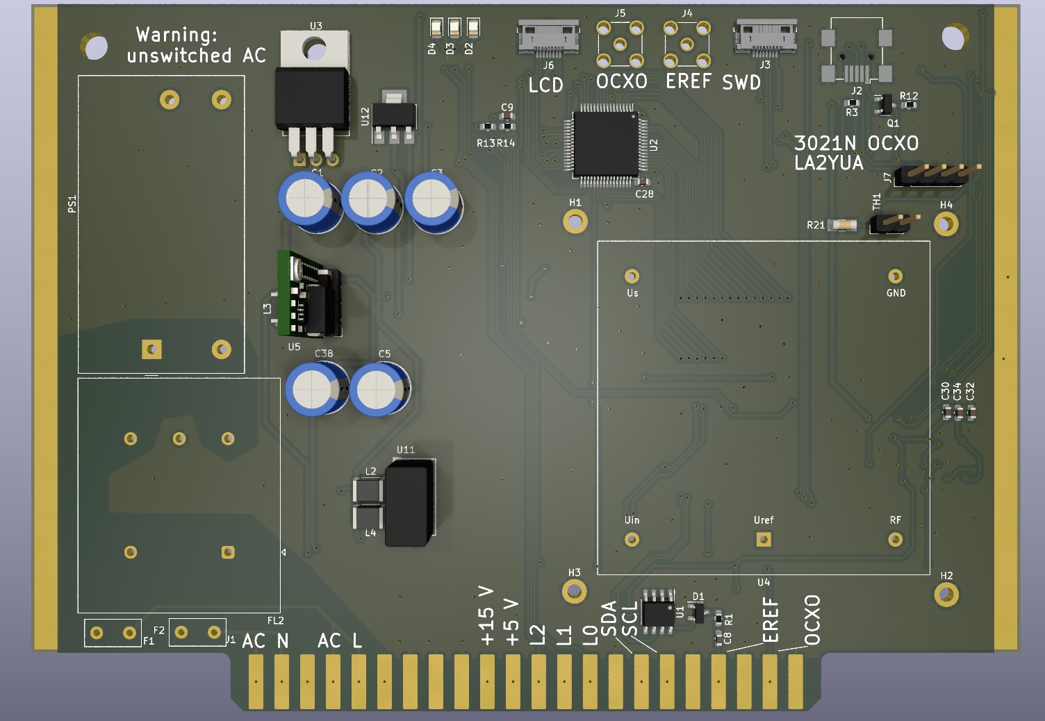
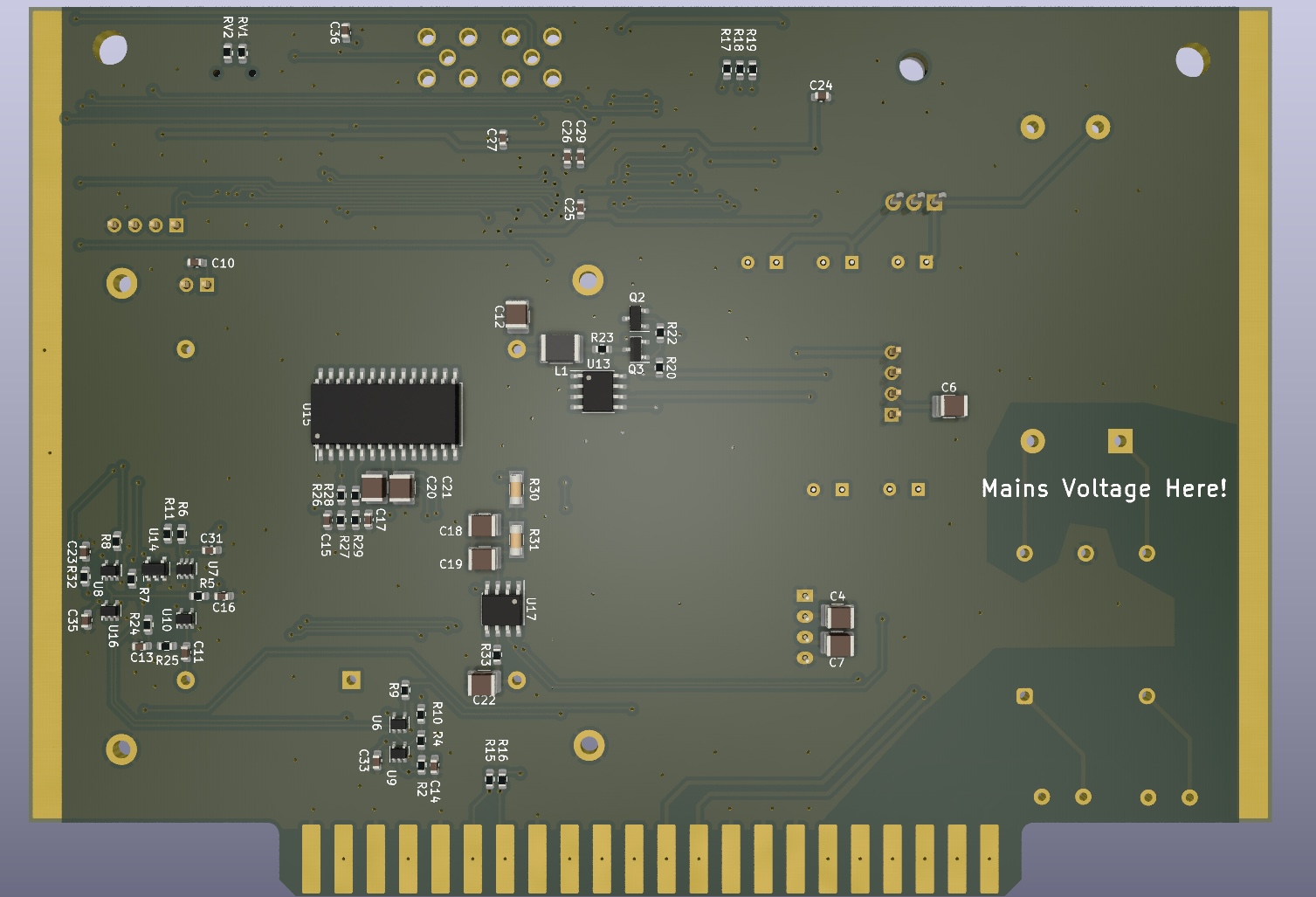
An external 220 V AC power supply is tapped off before the main power switch to allow continuous operation. A 10 W 15 V power supply is used to power the system, this will be relatively heavily loaded during warmup but idle state dissipation is quite low.
The OCXO runs off 12 V, but I added a 7812 regulator to keep the 12 V stable with low ripple. A DC/DC converter makes a 5 V supply, and another DC/DC makes a –12 V supply for the DAC.
The OCXO is the same C-MAC type as described previously, the same DAC is used, and the same BIT test system was integrated.
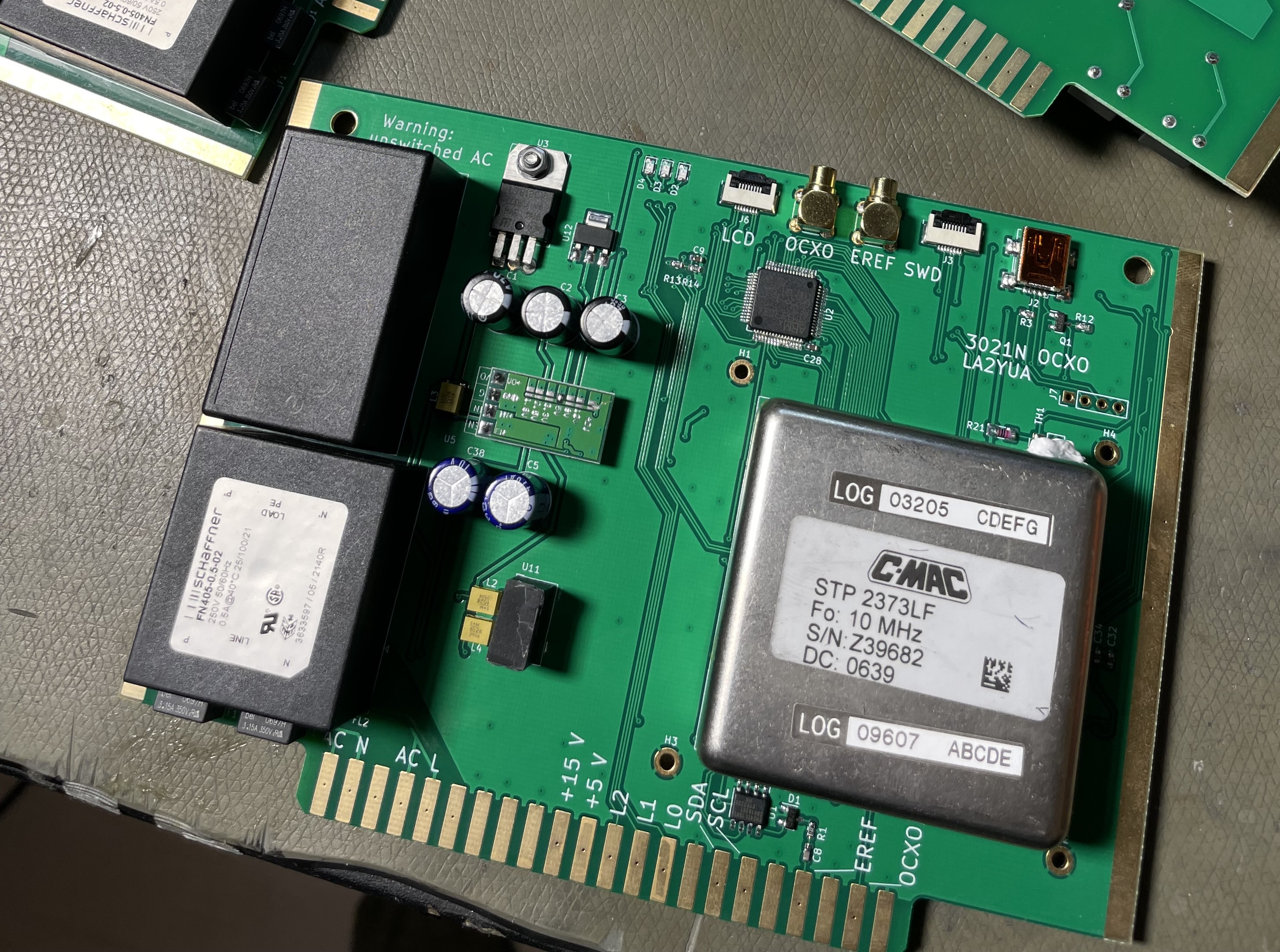
A 3D printed PolyCarbonate (PC) lid was also added over the OCXO to reduce the effects of convection or forced air cooling. This lid has a foam gasket to the PCB and has around 1-2 mm air gap around the entire OCXO. This was manufactured by PCBWay (my first 3D print order there), and the PC material was selected for it's acceptable price and high max operating temperature.
A STM32F103RET6 was used as the controller, which controls the 16 bit DAC with dithering to tune the OCXO. F-RAM storage is used for permanent storage of tuning voltage and unit parameters.
I failed to notice that the USB peripheral requires an 8 MHz input clock, I did make an adapter PCB to correct this with a PLL circuit but this has not been integrated at the time of publication.
FLL/PLL
The biggest difference between the previous smart OCXO and this implementation is the addition of frequency locked and phase locked loop (FLL & PLL) modes. The OCXO connects to the rear panel 10 MHz input, and this signal is divided down by 1024 and the frequency of this can be measured by the MCU, which is clocked from the OCXO.
This allows for highly precise but slow frequency measurement, and a frequency locked loop can be implemented to control the frequency very slowly. The only issue here is that the minimum frequency error is finite, and given by the integration time. The OCXO may therefore end up locked with some tiny frequency error that is never fully removed.
To support phase locking of the 10 MHz input, a basic XOR gate compares the two 10 MHz input signals after some division, and the output of this XOR gate is low pass filtered and sampled by the ADC. This allows for a direct phase measurement, keeping the phase stable makes it impossible to have any net long term frequency error since the phase error is the integral of the frequency change.
The XOR detector will lock at around 90° phase offset, but this isn't really a problem in this application.
XOR phase measurement also requires the OCXO frequency to be very close to the correct frequency for the phase measurement to yield good measurements. This is ensured in this case (where locking speed is irrelevant) by using the FLL as the first stage locker.
When an XOR gate is used to control a VCO, the bandwidth of the low pass filter between the XOR gate or mixer output and the VCO must be higher than the absolute frequency difference between the inputs.
In order to achieve high stability locking, a state machine measures loop error signals (RMS phase error, and RMS phase-derivative) and decreases the PLL bandwidth in stages. If a frequency or large phase error is accumulated for some reason, the state machine will decrement and increase the bandwidth until it is able to reacquire the signal.
Further, if the highest bandwidth mode is reached and the phase error is large, the PLL integrator is reset based on the frequency measurements periodically. This requires knowledge of the OCXO tuning gain, and when tuned correctly it is able to relatively quickly acquire any input frequency.
If the frequency measurement error exceeds the tuning range of the OCXO (around 20 Hz), the input is considered invalid and holdover mode is set instead.
When the lowest loop bandwidth state is reached, the system is considered stable, and after around 10 minutes it will begin storing tuning data to F-RAM. This mode has such a low integral gain that it's basically only able to correct for local OCXO drift, so any real change in the reference frequency will trigger a bandwidth increase. The idea is that the PLL integrator level will represent a good long term average of the correct tuning.
Test Experiences
This mode of regulation is fairly selective, and e.g. a TCXO equipped LEA-M8F clock is the "bad" reference clock I used for testing. This tends to wander back and forth over a period of 10-20 seconds. The phase error is not so tremendous that it can't be used with confidence, but e.g. a PZF180PEX with OCXO has much better short term stability.
My LEA-M8F is TCXO equipped, but it can also be set up to control external OCXO's and similar, which would likely improve it significantly.
The difference between these is easily observed when locking this OCXO to one of them; the PZF180PEX will be very quickly acquired and will tend to stay in the locked state basically forever as long as the RF signal is present. Meanwhile the LEA-M8F does more weird stuff and wanders back and forth, which accumulates loop errors that occasionally triggers a bandwidth increase. Note that the PZF180PEX does wander when losing RF lock, but it does so quite slowly and mostly monotonically.
On my TODO list is making a phase-logging system to produce actual data, but at present I don't have an automatic logging system to give me quantitative data.
Interface
The other main change is the addition of a USB plug, which is used to implement a virtual COM port, and this is used for communications. At least it would be, if I had used a MCU core clock compatible with USB. A future modification will be to add a PLL clock generator to convert the 10 MHz MCU clock to 8 MHz, allowing for USB operation.
A FFC connector with a LCD interface was also added, this is meant to be used when using the OCXO card standalone as a frequency standard or jitter cleaner. It matches some previously made HD44780 LCD interface controller cards I have made for 2x40 character LCD displays.
On the back plane side the card outputs regulated 15 and 5 V supplies, 3 LED outputs (straight LVCMOS), and I2C.
Software
The software was ported from the Smart OCXO's and the already described FLL/PLL mode of operation was implemented. An LCD display output was added for use in standalone applications, and due to the USB issues this and the debugger are the only interfaces currently implemented.
Some LED outputs were also added to indicate status. Further, the tuning word for the OCXO is not automatically updated in the F-RAM unless the PLL/1PPS is in a stable and locked state.
Weird Bugs: F-RAM Addressing
A fun self-inflicted bug I found was caused by using the FM24CL16 F-RAM IC with the STM32 HAL HAL_I2C_Mem_Read/HAL_I2C_Mem_Write functions.
I store this double buffered, but the data structure used is larger than 128 bytes. Since I was using 8-bit mode this doesn't work, but since one entry would normally be fine it went unnoticed. I originally wrote the code to use smaller entries that would fit fine in the 8 bit address space.
(Might have been nice if the STM32 HAL checked if the address offset + access size would fit though.)
Also turns out that the FM24CL16 uses the lower 3 address bits for paging 8-bit addresses, which is not directly supported by the STM32 HAL.
So what I did was switch to store one entry per page, by offsetting the device address.
This bug was also present on the Smart OCXO.
Weird Bugs: STM32F103 I²C
The I²C controller on specifically the STM32F103 series has some issues that seem to be specific to it, the F0, F3, and F4 devices seem to be far better.
Basically it will tend to randomly fail, sometimes locking up with a HAL_BUSY flag that never goes away. This issue is documented in an errata, and the workaround is really horrible.
I also had a really strange issue where a memory block read would inject a random extra 0 byte on readback. This offset some data structures, which obviously weren't correct anymore.
I've found at least part of the fix is to add 10 pF capacitors across the SDA/SCL lines to VCC (or to ground).
Frankly I would suggest avoiding the F1 devices for I2C applications, it's just not worth the trouble. I spent a lot of time adding additional checks and checksums to the I2C routines that shouldn't have been necessary.
Weird Behaviour: STM32 PWM Input Capture
I use the STM32 PWM input capture interrupt mode to measure the external frequency after division. The counter operates at CPU core rates and measures the period and on-time of the external square wave.
Currently the system works on interrupts, and 1'000'000 samples are taken per measurement (takes around 100 seconds). The period measurement seems to consistently be 2 cycles less than the actual time.
While not documented anywhere I could find it seems that detecting the rising edge and latching the counter value takes 2 core cycles that are then lost.
Adding 2 cycles to each measurements seems to yield correct results.
Long Term Results
19" Rack Unit
An example of this PCA was installed in a 19" enclosure along with a small 10 MHz distribution amplifier and fiber-optic interface, and powered on continuously starting in late January 2023. During this time the rack was moved back and forth somewhat, and no particular care was taken to avoid vibration or other disturbances.
Prior to the test, the unit had been connected to an external reference for approximately 1 week, and as part of redecorating the fiber carrying the 10 MHz reference was removed leaving it on holdover for the duration. Power was maintained throughout the test, with an OCXO enclosure temperature settling at 58 °C ±1°.
August 2023 Spot Check
A spot check was carried out in August 2023 of the frequency relative to my LEA-M8F and PZF180PEX receivers.
Frequency errors were not measurable using my HP 5335A frequency counter, an oscilloscope measuring differential frequency showed a frequency error on the order of 1 cycle per several minutes. The phase-drift of the LEA-M8F makes even these oscilloscope measurements difficult for that comparison.
The unit was left running to continue the test, since no relevant frequency error was found.