FEI-Zyfer NanoSync I/II

This is a cute little clock intended for OEM precision timing, let's look at how it's built.
Introduction
The FEI-Zyfer NanoSync II is an obsolete GPS disciplined oscillator (GPSDO) with a 10 MHz sine wave output, as well as 1PPS, and RS-232 serial.
The device was introduced around 2002, and supported through at least 2008. In 2021 this device is not supported or even acknowledged by the manufacturer.
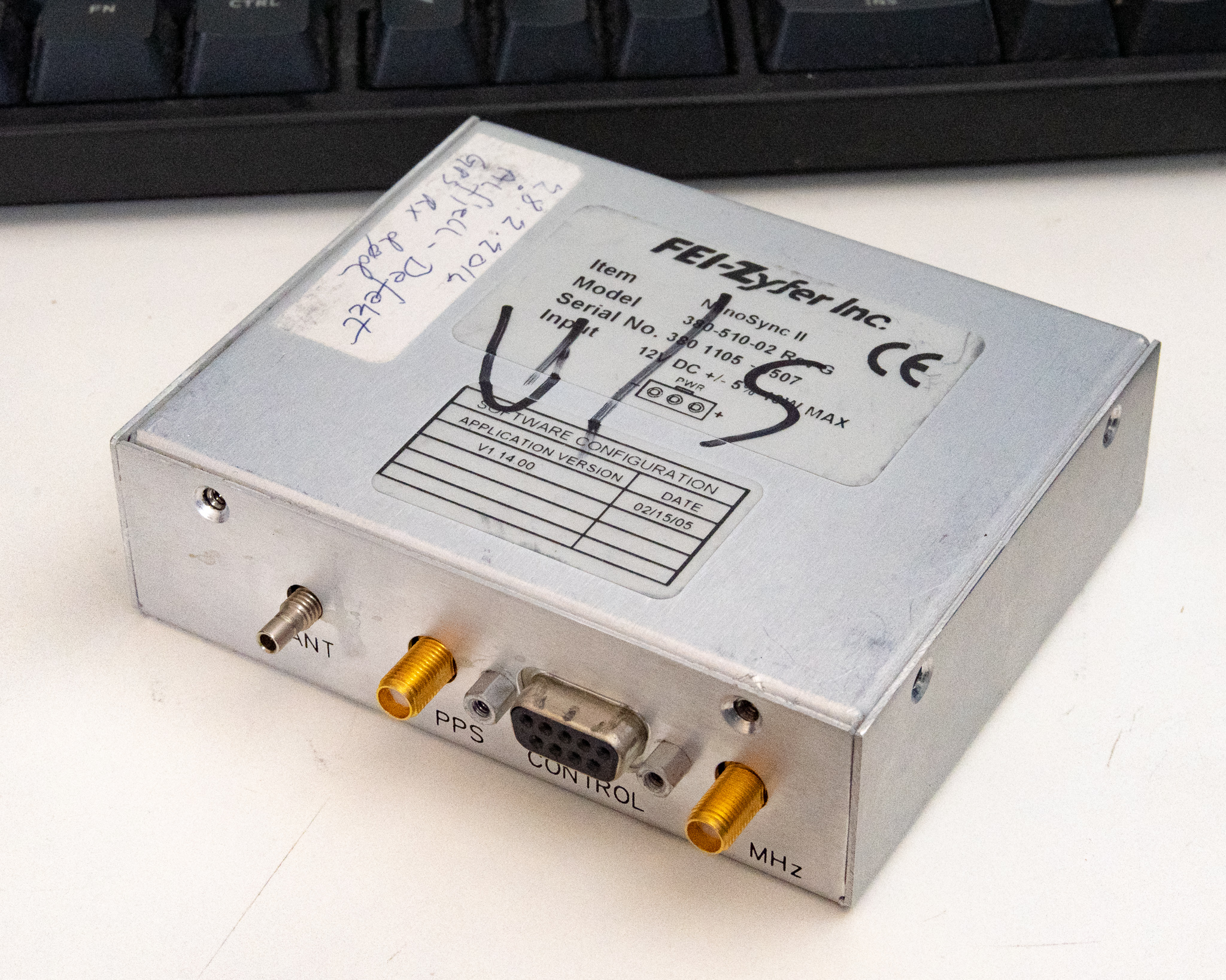
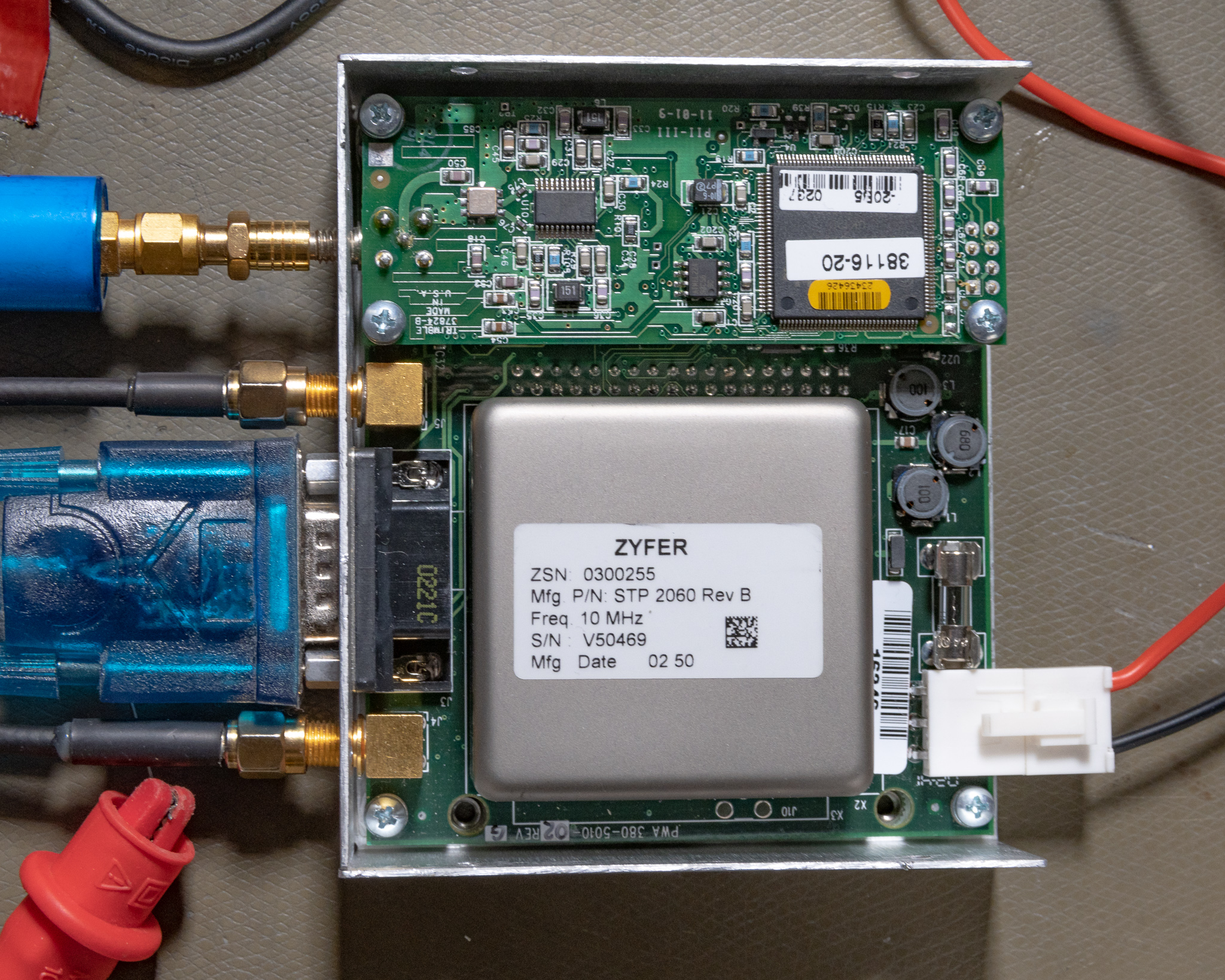
It's very compact, and clearly intended for integration into other devices. There are threaded insers (6-32 imperial thread) on 2.2 and 3.5" centers on the bottom (¼" max screw depth). The NanoSync II is slightly larger, but has the same mounting-hole footprint as the I version.
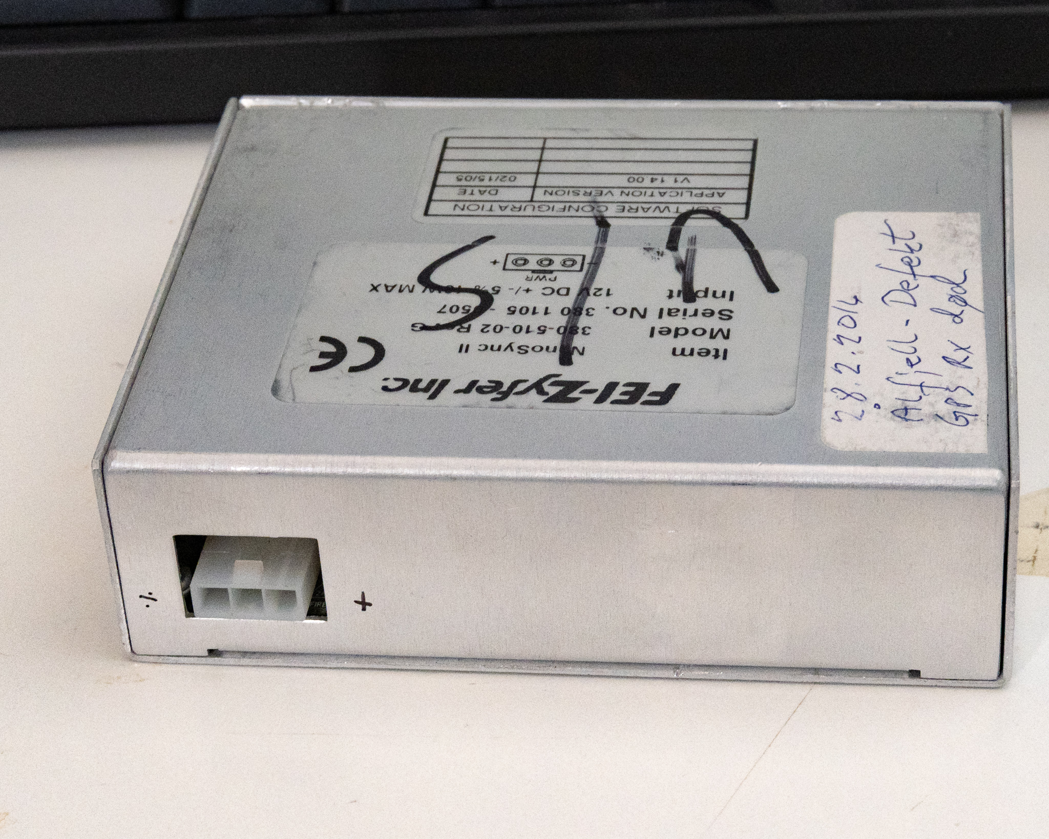
It runs off a 12 V supply using a 3 pin Molex type connector listed as 39-01-4031 (shell) and 39-00-0039 (female terminal). The pins are in the Mini-Fit series, the same kind used for PCIe power, and I suggest also buying the extraction tool part no. 11030044 since it's basically impossible to remove the terminals any other way. Power consumption is listed as around 5 W when operating and up to 12.5 W when warming up, which is quite reasonable.
The units I received were pulled from service due to faults, all units had a single oven OCXO, which is more advanced than the TCXO option, but not as nice as the double oven OCXO option.
Performance and Hookup
The specification for frequency error is 1·10–12, and after 12 hours operational the first device I tested gave a self-reported error of 3·10–13, which is in line with expectations. The NanoSync I measured against my LEA-M8F receiver system a HP 5335A gave an absolute frequency standard deviation of 3.6·10–3 Hz (fractional error of 0.36·10–9 at 10 MHz, 1000 samples at max integration time.
In this test the satellite reception wasn't amazing due to a somewhat weak signal from the antenna relative to what the receiver prefers, it will likely perform better with a high gain antenna.
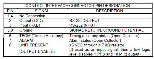
There is a standard serial port available, though with additional pins in use, which runs at 19200-8N1, using CR and LF as line feed characters. The device will on occasion print some info here on its own, and on startup it will print status info, but it quiets down after that. The serial port also has some discrete control lines, these are described in the user manual. I would suggest a useful mod could be to route the GPS UART to one of the unused pins, since the Trimble software is more convenient for GPS status monitoring.
The documentation is not easily found but is available in the web archive if you know where to look. The control software software isn't super critical, since the commands are relatively human readable (not as bad as the old Epsilon binary format).
A documentation package for the clock and some of the components can be downloaded here.
The official GpsMon application can be found here. It's not the happiest program ever written, but it does appear to work in Windows 10.
I made a little text file with some useful commands to paste into a serial terminal to monitor the clock status, and also dug up the original manual and serial command interface description through the web archive. I suggest issuing a factory reset command if you get one, just to normalize the settings.
GPS Time
The unit uses a GPS receiver made by Trimble, this is quite an old unit (as you can see from the low level of integration), introduced in 1999 or so. The numbers on the module are hard to track down, but turns out this is a "Lassen SK2" receiver (Trimble Studio IDs it as a "Lassen SK8-II".
This receiver is similar to the Motorola OnCore UT+ used in e.g. the Lucent RFTG-u's, in that it's a basic 8 channel L1 receiver. It's also similar in that it has very poor sensitivity and tracking ability when compared to e.g. a relatively modern LEA-M8F from uBlox. As such a high gain antenna is probably called for with this receiver. The Lassen was able to track 3 satellites while LEA-M8F could track 9 GPS L1 satellites with the exact same applied signal.
Unlike the UT+ receiver this receiver does not appear to support epoch-update, and as such due to GPS week rollover it thinks 2021 is actually 2002. This was apparently enough of an issue that a small market for Lassen SK2 clones appeared back in 2016.
The only major effect of this issue is that time of day output is off by some integer number of weeks, the time of day/1PPS is still valid, and the frequency stability is not affected. If you want to run a NTP server or similar you'll likely want to set up a microcontroller in series to offset the time to correct for this (and to rewrite the data into NMEA format). On startup the device outputs a time of 1980, day 6.
In Use
The specified startup time is minimum 8 hours, before this time the device can't enter holdover, and will likely jump a bit up and down as it adjusts its drift and thermal models. GPS almanac acquisition is quite slow with this GPS, and can easily take up to 1 hour before a good lock is reached.
A design issue with the unit in my opinion is that it doesn't have any LEDs to indicate lock status. This means that if some fault occurs it's very difficult to notice it unless you're polling the serial port for status info. By default, the 1PPS output is not active unless the device has reached lock status, I believe it stays active in holdover until some internal error estimate reaches a limit.
A mod to improve this situation would be to either hook up a LED + ⁄2 circuit to the 1PPS (giving a 1⁄2 Hz LED blinky when working), or hook up a LED directly to the 1PPS driver and configure the receiver to output a reasonably wide pulse (use the PULW command). The default pulse width is 2 ms. You could also use the ALARM and TFOM signals in the D-Sub to drive status LEDs.
Internals
The units had two different types of OCXO, the NanoSync I had a type made by Zyfer, and the NanoSync IIs used a Morion MV62 OCXO (this one you can get the datasheet for). The II's also have a small trim-cap next to the OCXO, presumably you can tweak this to affect the OCXO tuning?
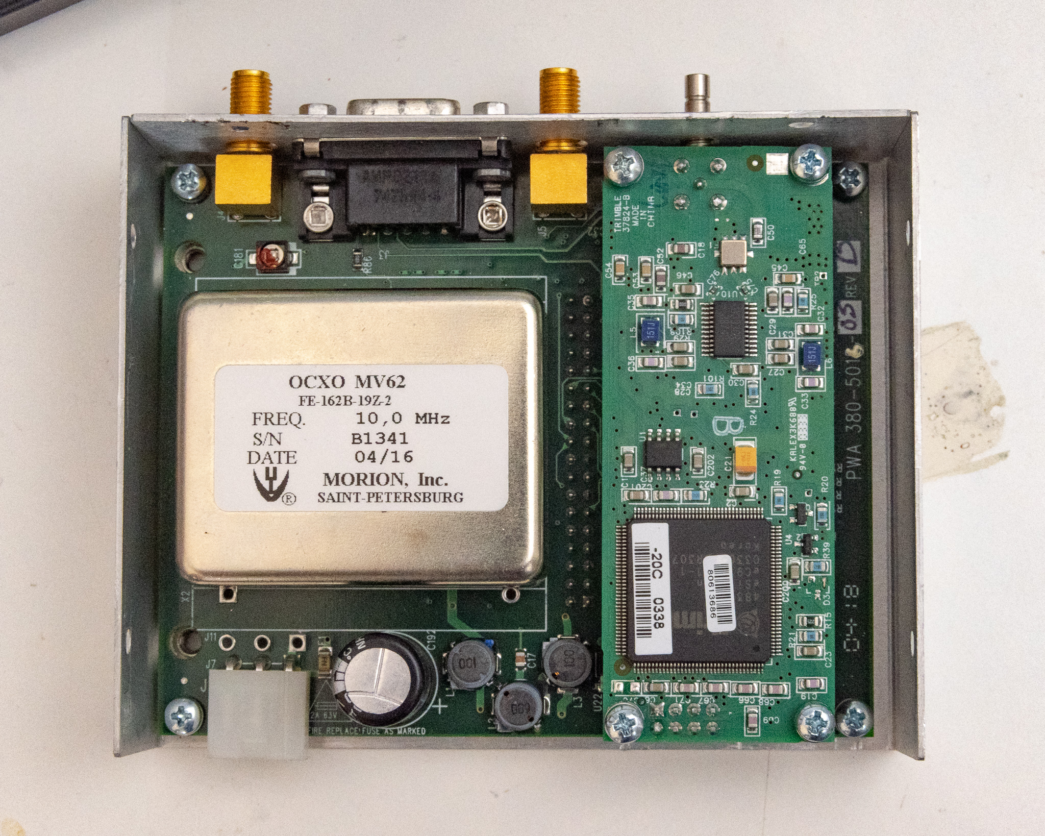
The Trimble GPS receiver appears to be a custom variant, since the stock unit has a sampling/RF reference TCXO which has been removed in this variant. Instead it looks like Zyfer put in a (possibly VC)TCXO on the main board and routed this onto the GPS board. Presumably this is done in an attempt to improve phase noise, since the sampling/RF oscillator can then be phase locked to the OCXO.
It also appears that they might in fact be using the GPS modules internal measurement of oscillator error to perform regulation; the GPS provides frequency error readings over serial that match the measured 10 MHz frequency offset on the output. This likely means that replacing the GPS module with a more modern one is likely very impractical. A possible benefit of this design is that the GPS module can do a more direct frequency error measurement, possibly allowing a faster acquisition time.
Both versions used the same Trimble receiver, the PCB is marked 37824-B.
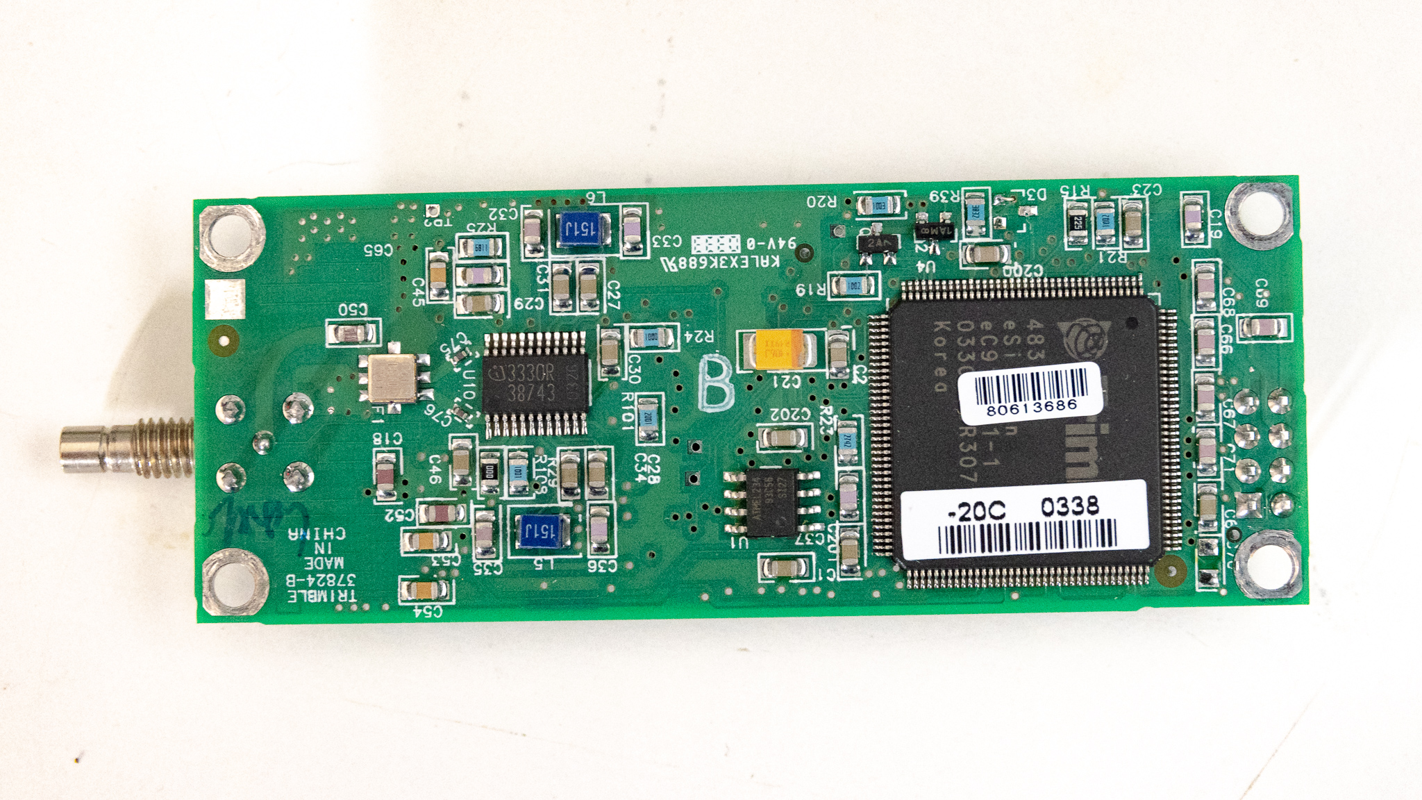
Ground is top right, serial data from the GPS is second from the bottom on the left.
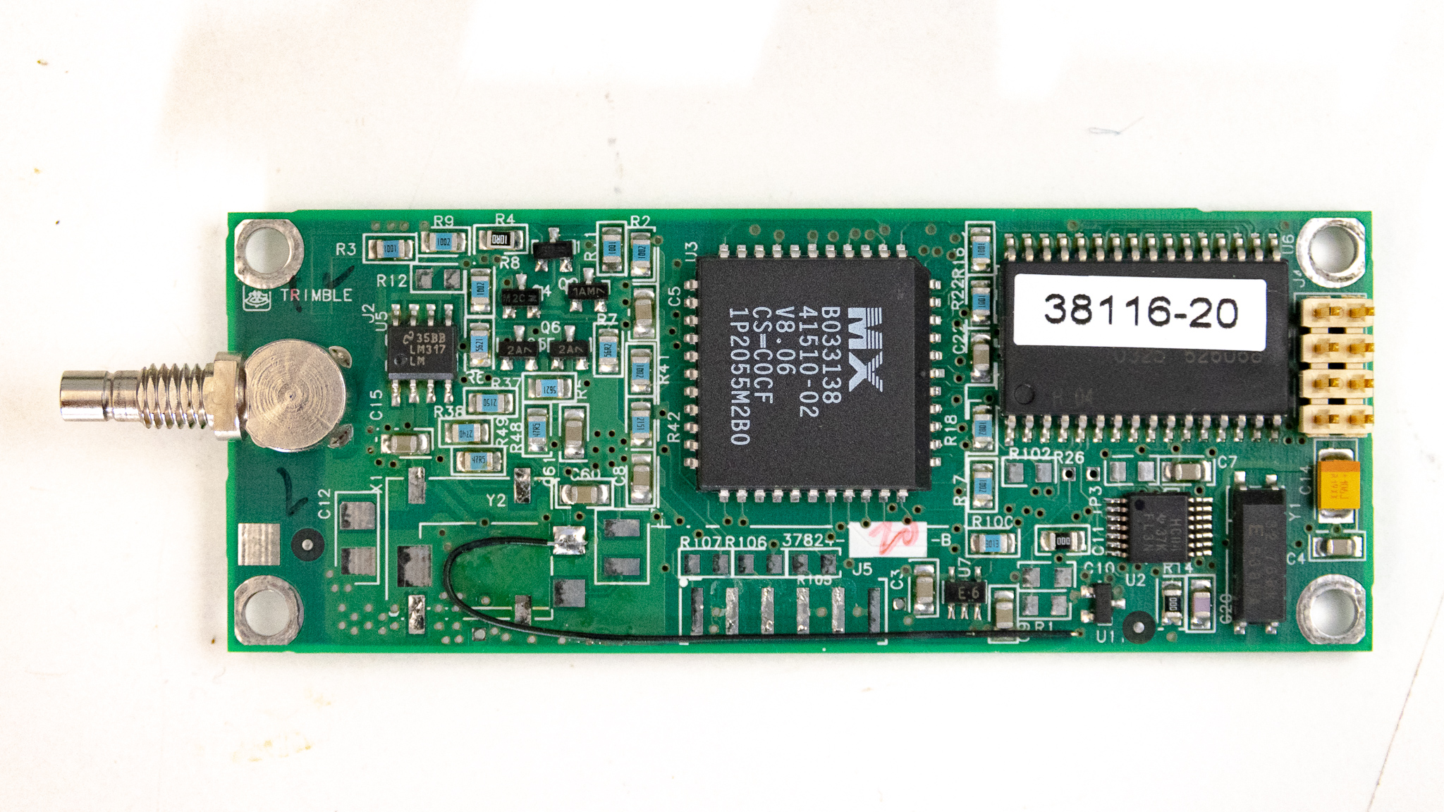
The failed transistors in the bias-circuit were the two upper-left ones (next to R8 and R4), the very top one is a BC807/2N2907 type, the one below and left is a BC857 or similar. R4 is the 10 Ω series resistor for the bias-circuit.
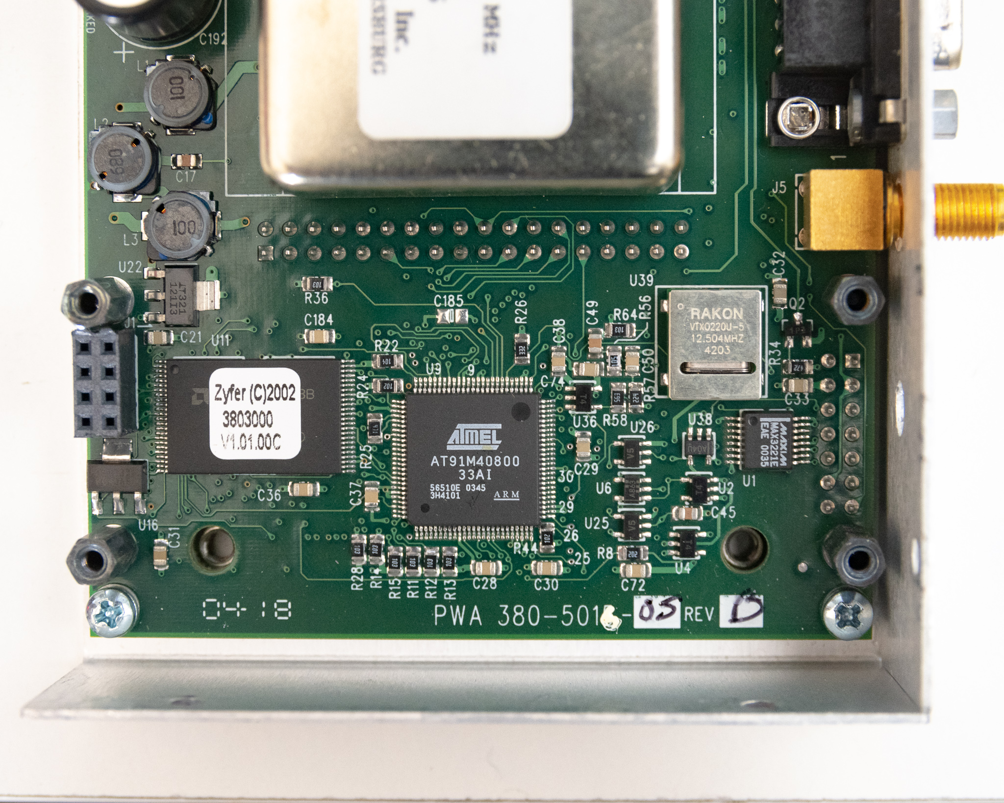
The main processor is an Atmel AT91 ARM microcontroller, and we can also see the external GPS reference crystal made by Rakon.
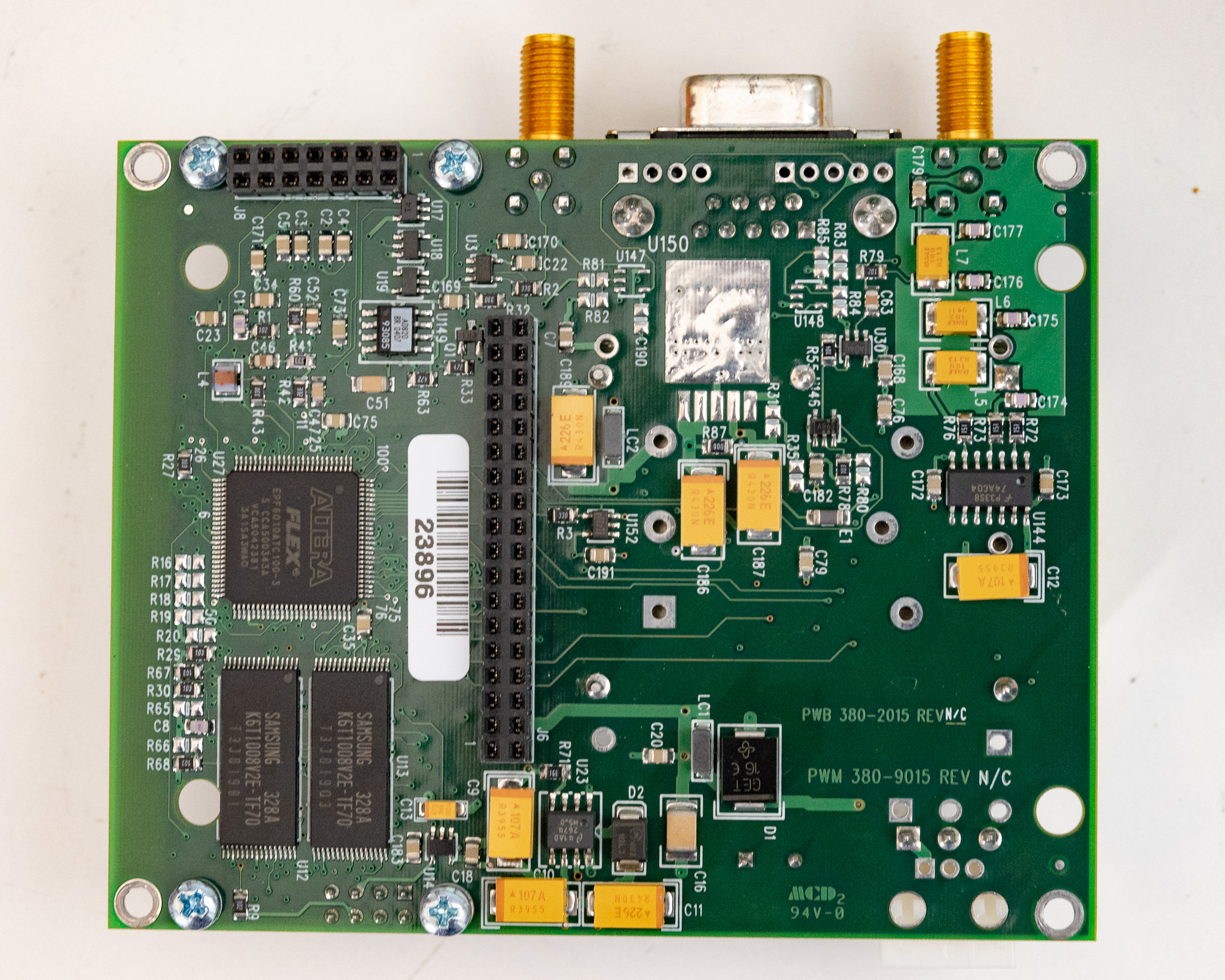
The main guts of the timing loop is an Altera Flex FPGA, and there appears to be some external SRAM for the FPGA or processor. The SRAM is part no. K6T1008V2E-TF70, it is a 128kx8 bit configuration with a 70 ns cycle time, the package is a 32 pin TSOP (wide type).eb
I couldn't immediately identify a DAC, it's possible the DAC is done using some type of PWM output from the FPGA, the AD820 opamp is likely what drives the OCXO trim voltage. I also don't see any obvious ADC for e.g. temperature measurement, this may be one of the SOT-23 devices, or perhaps built in to the FPGA? Probing around the FPGA appears to output some type of PWM/PDM type signal to pins going into that area of the board.
The AT91 doesn't appears to have any analog hardware built in.
We can identify that the 10 MHz output is generated using a 74AC04 hex inverter with at least 3 outputs in parallel, and a 7th order output low pass filter. The 1PPS output is generated by U3, which is probably a single-gate logic IC.
Troubleshooting
The first unit I tried was mostly working, the only issue I could find was that the GPS antenna port only had 0.6 V bias voltage on it, instead of the 4-5 V you'd expect.
This turned out to be caused by two failed PNP transistors on the GPS board. The GPS board is only specified for a measly 25 mA, rather than the more common 50-100 mA modern units can provide. Many antennas can pull more than this, and I suspect the failure occurred due to a persistent antenna overload.
Both PNP transistors were successfully swapped to BC857Cs, since that's all I had available, and I was able to hook up an amplified fiber optic receiver to connect to my grand unified receiver system and get a frequency lock.
One of the transistor is basically a BC857, while the other is a BC807 according to markings, this is similar to a 2N2907, rated for 500 mA collector current.
The two NanoSync II devices I tried appeared to have some random glitchyness. This glitchyness appears to have been caused by a poorly performing USB UART adapter, as the output later was verified to be ok with a logic analyzer.
What solved this issue was making a serial-adapter cable that only connected pins 2, 3, and 5. I suspect some of the non-standard voltages on the other pins caused issues for the serial adapter (the high/low voltages on the serial pins were way off with it connected).
It seems like the NanoSync IIs are different in this regard. The full boot sequence takes around 15 seconds.
With a TTL UART adapter we can monitor the GPS receiver with Trimble Studio. The GPS runs at 9600-8O1, and outputs in TSIP binary format. Trimble Studio v1.08 was able to give me a useful status output.
Two of the three clocks I tested only appeared to have the GPS bias issue, the last one did not have the bias issue. It appears this device had very poor sensitivity to GPS signals, and it also on one occasion reported a DAC value of UINT32_MAX after a while. This is far outside the valid range of 0-65535, and I suspect some issue with the SRAM or perhaps the AT91 processor.
The poor selectivity is most likely could have been a damaged SAW filter on the antenna-input; the owner reported it's not uncommon for lightning to strike near the antennas and this could cause filter damage.
My plan is to attempt to replace the RAM chips, as these are not particularly expensive or hard to replace. To determine if the GPS SAW filter is defective: a S11 measurement with a NanoVNA v2 and comparing to a working specimen will likely reveal if there is any reason for concern.
Update: S11 measurements of the GPS port found no differences between a working and non-working unit. RAM replacement also made no difference.